Alumina 96% Al2O3 metallization is compatible with every major bonding method in electronics: thick film, thin film (sputtered seed + plating, i.e., DPC), direct bonded copper (DBC), and active metal brazing (AMB). The 4% glassy phase in 96% alumina makes it the easiest ceramic to metallize, accepting a wider range of processes than purer grades or aluminum nitride. The best alumina 96% Al2O3 metallization route for your board depends on required copper thickness, trace resolution, adhesion strength, and thermal budget. This article compares all four routes so you can pick the right one.
Key Takeaways
- 96% alumina accepts thick-film, thin-film/DPC, DBC, and AMB metallization—more options than any other ceramic substrate.
- Thick-film screen printing fires at 850–950 °C and delivers 8–15 µm conductor layers with adhesion of 20–40 N/cm² (per IPC-TM-650 2.4.21).
- DPC (sputtered Ti/Cu seed + electroplated copper) achieves trace/space down to 30–50 µm on 96% alumina, with copper thickness from 1 µm to roughly 100 µm.
- DBC bonds 150–600 µm copper foil to alumina at 1065–1083 °C using the Cu–O eutectic, with peel strength typically >60 N/cm.
- AMB uses an active solder (commonly AgCuTi) at 780–900 °C and can bond copper up to 800 µm, but costs 2–4× more than DBC for the same footprint.
Why Alumina 96% Al2O3 Metallization Is Straightforward
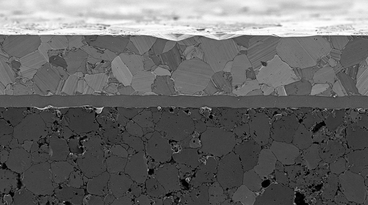
The 4% glassy phase in 96% Al2O3 (typically SiO2–CaO–MgO) plays a critical role. During thick-film firing, the glass frit in the paste reacts with this glassy grain boundary, forming a chemical bond that anchors the conductor. Purer grades like 99.6% alumina have almost no glassy phase, which makes thick-film adhesion weaker and shifts preference toward thin-film or brazing methods.
For DBC, the Cu₂O layer that forms during the eutectic bonding process wets the alumina surface well because the surface energy of polycrystalline 96% Al2O3 (measured at roughly 900–1000 mJ/m² per CoorsTek data) is high enough to support oxide wetting. Surface roughness matters: Ra of 0.3–0.8 µm (as-fired) is typical for 96% alumina and generally adequate for DBC and thick film without additional lapping or grinding of the ceramic substrate. Thin-film sputtering, by contrast, often benefits from polished surfaces (Ra < 0.1 µm) to achieve uniform seed layers.
Alumina 96% Al2O3 Metallization Methods Compared
| Parameter | Thick Film | Thin Film / DPC | DBC | AMB |
|---|---|---|---|---|
| Conductor material | Au, Ag, AgPd, Cu | Cu (Ti or TiW adhesion layer) | Cu foil (OF-Cu) | Cu foil (OF-Cu) |
| Copper thickness range | 8–15 µm (printed) | 1–100 µm | 150–600 µm | 150–800 µm |
| Min trace / space | 100–150 µm | 30–50 µm | 300–500 µm | 300–500 µm |
| Process temperature | 850–950 °C | <250 °C (sputter + plate) | 1065–1083 °C | 780–900 °C |
| Adhesion (peel / pull) | 20–40 N/cm² pull | 5–15 N/cm peel (Ti/Cu on polished Al2O3) | >60 N/cm peel | >80 N/cm peel |
| Thermal conductivity of bond | Limited by glass frit layer | Near-bulk Cu | Near-bulk Cu | Limited by braze interlayer (~2–5 µm) |
| Typical application | Hybrid circuits, resistor networks | LED, RF, sensor | Power modules (IGBT, SiC) | High-reliability power (EV, traction) |
Typical values for commercially available material, for comparison only. Confirm against the datasheet for your specific grade.
Thick-Film Metallization on 96% Alumina
Thick-film screen printing is the oldest and lowest-cost alumina 96% Al2O3 metallization route. A conductor paste (e.g., DuPont QM44 or Heraeus C1076) is printed through a stainless-steel mesh, dried at 100–150 °C, then fired in a belt furnace at 850–950 °C for 8–12 minutes at peak. The glass frit in the paste melts, wets the alumina’s glassy grain boundary, and resolidifies as an anchor layer roughly 1–3 µm thick.
Adhesion depends heavily on surface cleanliness. Organic contamination from handling or laser marking can drop pull strength by 30–50%. A proper cleaning and surface preparation step before printing is essential. Thick film is the go-to process when you need embedded resistors (cermet pastes) alongside conductors, or when the design only requires moderate line resolution.
Thin-Film / DPC Metallization on 96% Alumina
DPC (Direct Plated Copper) starts with vacuum sputtering of an adhesion layer—typically 50–200 nm of titanium or titanium-tungsten—followed by 200–500 nm of copper as a seed. The substrate then goes through photolithography and electroplating to build copper to the target thickness. For a deeper look at the seed-layer step, see sputtered seed layers in DPC metallization.
The advantage of DPC as an alumina 96% Al2O3 metallization method is resolution. Trace/space of 30–50 µm is routine, which makes it the default for LED thermal substrates, RF matching networks, and MEMS sensor packages. The Ti adhesion layer forms a thin TiO₂ interface with the alumina, providing a chemical bond rather than a mechanical one. Adhesion is lower than DBC or AMB in absolute terms but more than adequate for solder-reflow and wire-bonding loads. For specific DPC copper thickness and tolerance data, check the capability page.
Worked Example: DPC Trace Resistance on 96% Al2O3
Suppose you need a 50 µm wide, 10 mm long trace carrying 200 mA on a DPC alumina board with 20 µm plated copper. Resistivity of electroplated copper is approximately 1.8 × 10⁻⁸ Ω·m.
Cross-sectional area: 50 µm × 20 µm = 1,000 µm² = 1.0 × 10⁻⁹ m²
Resistance: R = ρL / A = (1.8 × 10⁻⁸ × 0.01) / 1.0 × 10⁻⁹ = 0.18 Ω
Voltage drop at 200 mA: 36 mV. Power dissipation: 7.2 mW. For most LED or sensor circuits this is negligible, but at higher currents you would widen the trace or increase copper thickness.
DBC and AMB on 96% Alumina
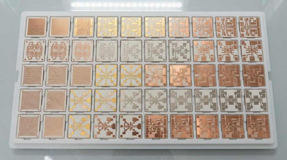
When the design calls for thick copper—150 µm and above—DBC and AMB are the two alumina 96% Al2O3 metallization options. DBC exploits the Cu–Cu₂O eutectic at 1065 °C to bond oxygen-free copper foil directly to the alumina surface. The process is well-proven for IGBT and SiC power modules. For layout constraints, refer to DBC layout guidelines.
AMB uses a reactive braze alloy containing titanium (commonly Ag-72Cu-28 + 1.5–4.5% Ti) at 780–900 °C under vacuum. The titanium reacts with alumina to form a TiO or TiN interlayer, creating a stronger bond than DBC. AMB is preferred for thermal cycling above 1,000 cycles at ΔT > 100 K, where DBC crack propagation at the Cu₂O interface becomes a reliability concern. The cost premium is significant—typically 2–4× per substrate—so AMB is reserved for automotive traction inverters, railway converters, and aerospace power stages where field failure is unacceptable.
When NOT to Use Alumina 96% Al2O3 Metallization
If your thermal dissipation exceeds roughly 50 W/cm² at the substrate level, the 24–28 W/mK thermal conductivity of 96% Al2O3 becomes the bottleneck regardless of metallization quality. Switch to aluminum nitride (170–200 W/mK). The metallization options for AlN differ; see how AlN substrates are metallized for a direct comparison.
If your circuit needs only single-sided copper with no fine features and operates below 130 °C, a metal-core PCB (aluminum MCPCB, 1–3 W/mK dielectric) costs 5–10× less per unit area. Use it instead.
If you require trace/space below 20 µm—common in mmWave GaN circuits above 40 GHz—thin-film on 99.6% alumina or AlN with a polished surface gives better line-edge definition than 96% alumina’s coarser grain structure (grain size 3–8 µm vs. 1–2 µm for 99.6%).
Frequently Asked Questions
Can you combine thick-film and thin-film metallization on the same 96% alumina substrate?
Yes. A common hybrid approach prints thick-film resistors first (fired at 850 °C), then sputters a thin-film conductor layer on top. The fired resistor withstands the sputter vacuum and subsequent plating chemistry. Sequencing matters: thick film fires first because its peak temperature would damage a pre-existing thin-film stack.
Does 96% alumina need a surface finish after metallization?
Almost always. Bare copper oxidizes within hours. Typical finishes on metallized alumina include ENIG (3–5 µm Ni, 0.05–0.1 µm Au), ENEPIG, OSP, or immersion silver, depending on the soldering or wire-bonding method. The finish choice follows the same rules as organic PCBs.
What adhesion test should I specify for metallized 96% alumina?
For thick film, specify a pull test per ASTM F1842 or IPC-TM-650 2.4.21 with 2 mm × 2 mm pads. For DPC, DBC, and AMB, a 90° peel test per IPC-TM-650 2.4.8 is standard. Always state the test method on your drawing; “good adhesion” without a number is not a spec.
Is 96% alumina compatible with co-fired metallization (HTCC or LTCC)?
Standard 96% Al2O3 substrates are pre-sintered (fired at ~1600 °C). They are not green tape and cannot be co-fired. HTCC uses high-purity alumina green tape with refractory metal (W, Mo) co-fired at 1500–1600 °C. LTCC uses a glass-ceramic tape system fired below 900 °C. These are distinct product families, not interchangeable with post-fire metallization of a finished 96% alumina substrate.
How does the glassy phase in 96% alumina affect high-frequency performance?
The SiO2-rich glassy phase increases dielectric loss. At 1 MHz, 96% Al2O3 has a loss tangent of roughly 0.0002–0.0010 (per Kyocera A-493 datasheet), while 99.6% alumina drops to 0.0001–0.0003. Above 10 GHz the difference becomes measurable in insertion loss. For mmWave circuits, 99.6% or AlN is the better substrate.
Next Step
If you have a design that needs metallized 96% alumina, review the full metallization capabilities and tolerances page to confirm your trace width, copper thickness, and adhesion requirements are within range. Then upload your files for a quote.