Aluminum nitride AlN metallization is the process of bonding a conductive metal layer—almost always copper—to an AlN ceramic substrate so it can carry current and transfer heat in power electronics, RF modules, and high-brightness LEDs. AlN’s thermal conductivity of 170–200 W/m·K (per Kyocera and CoorsTek datasheets, measured at 25 °C per ASTM E1461) makes it the go-to ceramic for high heat flux, but its covalent bonding and native surface oxide make metal adhesion harder than on alumina. The aluminum nitride AlN metallization method you choose determines adhesion strength, minimum feature size, copper thickness, and ultimately the thermal and electrical performance of the finished board.
Why Aluminum Nitride AlN Metallization Is Harder Than Alumina
Alumina (Al₂O₃) has a naturally rough, oxygen-rich surface that copper oxide wets easily during direct bonding. AlN is different. Its surface forms a thin aluminum oxynitride layer that is chemically stable and poorly wetted by copper at typical DBC process temperatures. Without pretreatment—oxidation annealing, plasma activation, or a reactive interlayer—copper simply will not adhere reliably.
This surface chemistry issue is the reason multiple metallization routes exist for AlN. Each one solves the adhesion problem differently, with distinct trade-offs in layer thickness, patterning resolution, and production cost. Understanding these trade-offs is essential before committing to a ceramic thermal management approach for your design.
Four Aluminum Nitride AlN Metallization Methods
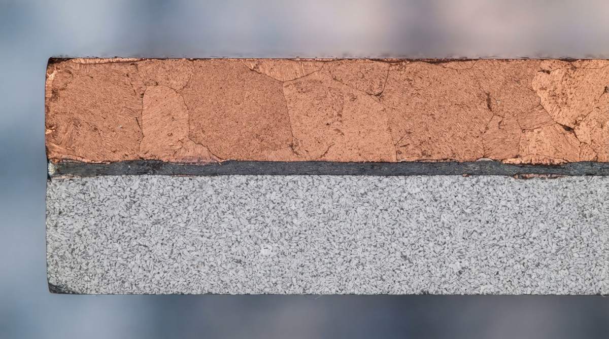
Direct Bonded Copper (DBC)
DBC bonds a copper foil to AlN through a thin copper-oxide eutectic layer formed at roughly 1065–1083 °C in a controlled atmosphere. On alumina, this process is straightforward. On AlN, a pre-oxidation step at 1100–1300 °C is needed to grow a sufficient alumina interlayer on the AlN surface so the Cu-O eutectic can wet it. This extra step adds process time and can introduce micro-cracks at the AlN–Al₂O₃ interface if not carefully controlled.
Typical DBC on AlN yields copper thicknesses of 0.15–0.50 mm, with peel strength in the range of 4–8 N/mm (per CeramTec and Kyocera published data). It is the most cost-effective high-current metallization for AlN when minimum feature size is above roughly 0.3 mm. For DBC design rules and tolerances, the substrate pre-oxidation quality is the critical variable.
Active Metal Brazing (AMB)
AMB uses a braze alloy containing an active element—typically titanium—that reacts directly with the AlN surface to form a TiN bonding layer. This eliminates the need for pre-oxidation entirely. Brazing temperatures are lower than DBC, usually 800–900 °C, and the resulting bond strength is higher: 8–15 N/mm peel strength is common, per Rogers/Curamik and Heraeus datasheets.
AMB supports thicker copper (0.3–1.2 mm) and produces joints that survive more aggressive thermal cycling. For AlN substrates in IGBT modules or SiC power converters—where ΔT can exceed 150 °C per cycle—AMB is the preferred route. The trade-off is cost: the active braze alloy is expensive, and the vacuum or inert-atmosphere furnace cycle is slower. See AMB copper thickness and capabilities for process limits.
Direct Plated Copper (DPC)
DPC starts with a sputtered adhesion layer (typically Ti or Cr, 20–100 nm) followed by a copper seed layer (200–500 nm), then electroplates copper to the target thickness—usually 10–150 µm. The sputtered titanium reacts with the AlN surface at the atomic level, giving excellent adhesion without high-temperature bonding.
DPC is the method of choice when you need fine features. Minimum trace and space below 50 µm is achievable, making DPC the standard for RF circuits on AlN and for LED submounts with dense wire-bond pads. Copper is thinner than DBC or AMB, so DPC is not suited for carrying hundreds of amps. For patterning constraints, refer to the DPC design rules for ceramic PCBs.
Thin-Film Sputtering (Without Plating)
For applications needing only a few microns of metal—resistor networks, microwave transmission lines, sensor electrodes—thin-film sputtering alone may suffice. A typical stack is Ti/Pt/Au or Ti/Ni/Au, deposited by PVD and patterned by photolithography and lift-off or wet etch. Adhesion strength exceeds 20 MPa (ASTM D4541 pull test). The limitation is current capacity: a 2 µm gold layer on a 50 µm trace carries milliamps, not amps.
How to Choose the Right AlN Metallization Process
Selecting the right aluminum nitride AlN metallization process comes down to four design parameters. Run through this checklist before requesting quotes:
- Current requirement: If the trace must carry more than 10 A, you need DBC (≥0.15 mm Cu) or AMB (≥0.3 mm Cu). DPC and thin-film are too thin.
- Feature size: Traces or spaces below 0.3 mm rule out DBC and AMB. Use DPC for 30–75 µm features, or thin-film sputtering for sub-25 µm.
- Thermal cycling severity: For ΔT above 100 °C over thousands of cycles, AMB’s higher peel strength (8–15 N/mm) and crack resistance outperform DBC.
- Budget: DBC costs roughly 1× baseline per unit area. AMB runs 1.5–2.5×, DPC 1.2–1.8×, and thin-film 1.5–3× depending on the metal stack.
- Wire bonding: If the design requires Au ball bonds, DPC or thin-film delivers the surface finish and roughness (Ra < 0.3 µm) needed without extra polishing.
AlN Metallization Methods Compared
| Parameter | DBC | AMB | DPC | Thin-Film Sputter |
|---|---|---|---|---|
| Copper thickness | 0.15–0.50 mm | 0.3–1.2 mm | 10–150 µm | 0.5–5 µm (Au or Cu) |
| Min. trace/space | ~0.3 mm / 0.3 mm | ~0.4 mm / 0.5 mm | 30–75 µm / 30–75 µm | 10–25 µm / 10–25 µm |
| Peel strength (N/mm) | 4–8 | 8–15 | 3–6 | N/A (pull test >20 MPa) |
| Process temp. | 1065–1083 °C | 800–900 °C | <200 °C (sputter + plate) | <200 °C |
| Pre-oxidation needed? | Yes | No | No | No |
| Thermal cycling reliability | Good | Excellent | Good (thin Cu) | Limited (thin layer) |
| Relative cost per unit area | 1× | 1.5–2.5× | 1.2–1.8× | 1.5–3× (depends on metals) |
Typical values for commercially available material, for comparison only. Confirm against the datasheet for your specific grade. Peel strength per IPC-TM-650 2.4.8. Sources: CoorsTek, Kyocera, Rogers/Curamik, Heraeus published data.
Worked Example: Choosing a Method for a 100 W SiC Half-Bridge
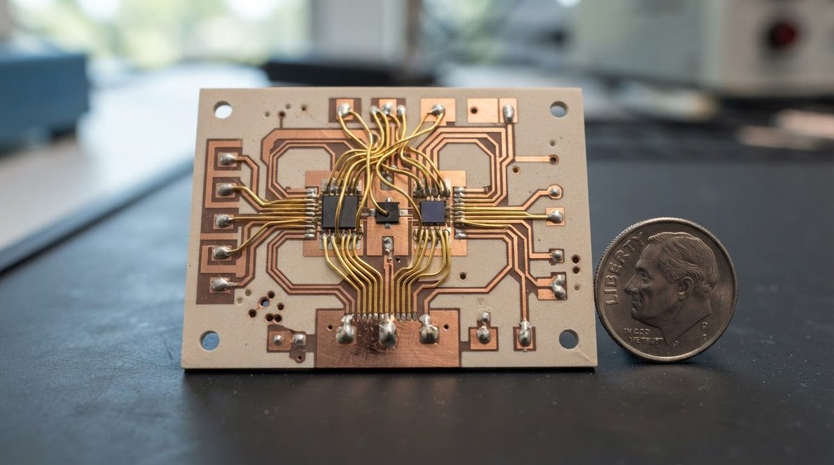
Suppose you need to mount two SiC MOSFETs dissipating 50 W each onto an AlN substrate. The drain pad is 8 mm × 10 mm, and the bus bar trace must carry 30 A continuous.
Thermal check: Through-substrate thermal resistance Rth = t / (k × A), where t = 0.635 mm (standard AlN thickness), k = 170 W/m·K, A = 80 mm² = 80 × 10⁻⁶ m². Rth = 0.000635 / (170 × 80 × 10⁻⁶) = 0.047 °C/W per die pad. At 50 W, that is only 2.3 °C rise through the ceramic. The bottleneck will be the solder joint and heatsink, not the substrate.
Current check: 30 A through a copper trace requires roughly 0.3 mm thick copper at 10 mm width to stay under a 20 °C temperature rise (per IPC-2152 charts for external conductors). DPC’s 150 µm maximum is too thin. DBC at 0.3 mm works. AMB at 0.3–0.8 mm works with margin.
Reliability check: SiC junction temperatures reach 175 °C, and thermal cycling from 25 °C to 175 °C will stress the Cu–ceramic interface. AMB’s higher peel strength and thicker copper make it the safer choice here, despite higher cost. If the product is consumer-grade with a shorter life target, DBC may suffice.
Verdict for this design: AMB with 0.3 mm copper on 0.635 mm AlN. Review the AMB design rules for minimum pad-to-edge clearance before layout.
Enter your substrate dimensions, copper thickness, and power dissipation below to estimate junction-to-case thermal resistance for your own AlN metallization stackup.
When Not to Use AlN Metallization
AlN substrates cost 3–5× more per unit area than 96% alumina. If your device dissipates under 10 W/cm² and operates below 150 °C, alumina with standard DBC or conventional ceramic metallization handles the job at a fraction of the price.
For applications above 300 W with extreme thermal cycling (e.g., traction inverters, railway converters), Si₃N₄ substrates with AMB may be a better fit. Si₃N₄ has lower thermal conductivity (70–90 W/m·K) but far higher fracture toughness (6–7 MPa·√m vs. 2.5–3.5 MPa·√m for AlN), making it more resistant to crack propagation under mechanical stress.
If your design needs only fine-pitch signal routing and no significant power, a standard FR-4 or Rogers high-frequency laminate is simpler and cheaper. Ceramic is not the default—it earns its place only when thermal, frequency, or reliability requirements demand it.
Frequently Asked Questions
Can you solder directly to metallized AlN?
Yes. All four aluminum nitride AlN metallization methods produce a solderable surface once a suitable finish is applied—typically Ni/Au (ENIG) or Ni/Ag. The nickel barrier prevents copper diffusion into the solder joint. Standard Pb-free solders (SAC305) and high-temperature solders (Au-Sn, Au-Ge) are both used on AlN substrates.
Does AlN metallization affect the substrate’s thermal conductivity?
The metallization itself does not change the bulk thermal conductivity of AlN (170–200 W/m·K). However, the interfacial bond layer—copper oxide in DBC, TiN in AMB, sputtered Ti in DPC—adds a small thermal boundary resistance, typically 0.01–0.05 °C·cm²/W. In most designs this is negligible compared to solder and TIM resistances.
What surface finish goes on top of the copper?
ENIG (electroless nickel / immersion gold) is the most common: 3–5 µm Ni + 0.05–0.1 µm Au. For wire bonding, thicker gold (0.5–1.0 µm electrolytic Au over Ni) is standard. Silver finish is used in some power module designs for cost reasons, but it requires passivation to prevent tarnish.
How do I specify AlN metallization on a drawing?
Call out the substrate material (AlN, with purity—typically ≥98%), substrate thickness, metallization method (DBC/AMB/DPC/thin-film), copper thickness, and surface finish. Include a cross-section stackup note. Reference IPC-6012ES (Qualification and Performance Specification for Rigid Printed Boards, Space and Military Avionics Applications) or the manufacturer’s design guide for tolerance classes.
Is AlN metallization compatible with wire bonding?
Yes. Both aluminum wedge bonding and gold ball bonding work on properly finished AlN substrates. The critical factor is the top metal finish: gold thickness must be ≥0.5 µm for reliable Au ball bonds, and surface roughness (Ra) should be below 0.3 µm. DPC and thin-film methods typically meet this without extra processing; DBC and AMB surfaces may need polishing or an additional plated finish. See copper plating for ceramic PCBs for post-bond plating options.
Next Step
If you have a specific AlN design in progress, gather your substrate thickness, copper weight, minimum feature size, and expected thermal cycle profile. These four parameters narrow the aluminum nitride AlN metallization choice to one or two methods. For copper-metallized AlN substrates ready to quote, upload your files and receive pricing within 24 hours.