The EV power module AlN PCB is the preferred ceramic substrate for traction inverters because aluminum nitride combines high thermal conductivity (170–200 W/mK) with a coefficient of thermal expansion (4.5 ppm/°C) closely matched to silicon carbide and silicon die. That combination lets traction inverters push 200+ A through a compact footprint without cracking solder joints or overheating junctions during aggressive drive cycles.
Key Takeaways
- An EV power module AlN PCB conducts heat 6–8× faster than a 96% alumina substrate (24–28 W/mK), reducing junction-to-case thermal resistance by 40–60% in a typical half-bridge module.
- A CTE of 4.5 ppm/°C sits between silicon (2.6 ppm/°C) and copper (17 ppm/°C), limiting thermo-mechanical stress on die-attach and solder layers during –40 °C to +175 °C cycling.
- Direct Bond Copper (DBC) and Active Metal Brazing (AMB) on AlN both survive 3,000+ thermal-shock cycles (–55 °C / +150 °C, per MIL-STD-883 Method 1010), though AMB offers higher copper peel strength.
- AlN substrates cost 3–5× more per unit area than 96% alumina, so they are justified only when thermal or CTE requirements cannot be met by lower-cost ceramics.
Why EV Power Module AlN PCB Substrates Dominate Traction Inverters
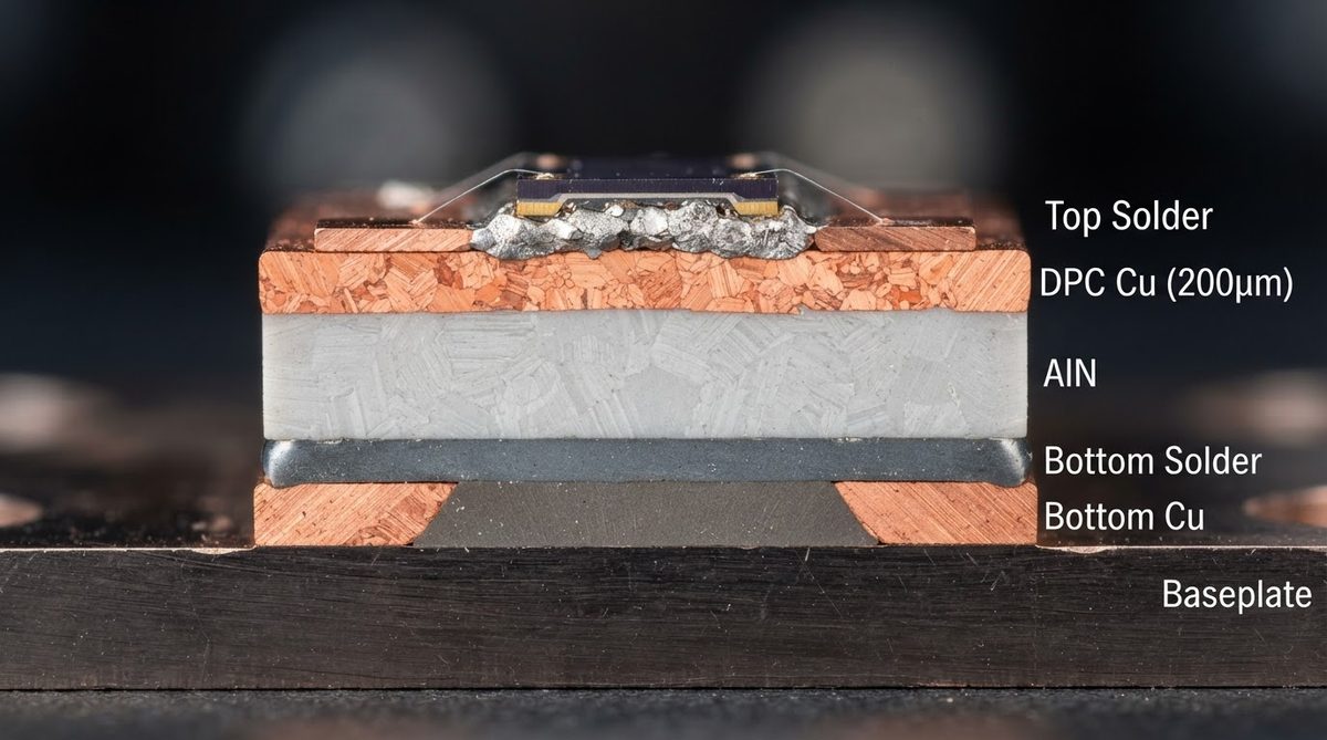
An EV traction inverter converts DC battery voltage (typically 400 V or 800 V) into three-phase AC for the drive motor. Each switching leg contains SiC MOSFETs or silicon IGBTs that dissipate 50–300 W per die during peak torque. Junction temperatures can reach 175 °C for SiC devices and 150 °C for silicon, while coolant on the opposite side of the substrate sits at 65–80 °C. The substrate must move that heat flux—often 100–200 W/cm²—without exceeding the die’s maximum junction temperature.
Alumina (Al₂O₃ 96%) works for lower-power industrial drives, but its 24–28 W/mK conductivity creates a thermal bottleneck at EV power densities. AlN closes that gap. At 170–200 W/mK (per Kyocera SH-30 and Maruwa AN series datasheets, measured at 20 °C), a 0.635 mm AlN substrate contributes roughly 0.03 °C·cm²/W to the thermal stack, compared to about 0.23 °C·cm²/W for the same thickness of 96% alumina. That difference directly lowers junction temperature or allows a smaller, lighter module at the same thermal margin. For broader context on how ceramic substrates manage heat in power electronics, see ceramic thermal management fundamentals.
Worked Example: Thermal Resistance Comparison
Consider a single SiC MOSFET die (5 mm × 5 mm, 150 W dissipation) soldered to a DBC substrate. The substrate thermal resistance through the ceramic layer is:
Rth,ceramic = t / (k × A)
Where t = thickness, k = thermal conductivity, A = die area.
| Parameter | 96% Al₂O₃ | AlN | Unit |
|---|---|---|---|
| Thickness (t) | 0.635 | 0.635 | mm |
| Thermal conductivity (k) | 26 | 180 | W/mK |
| Die area (A) | 25 | 25 | mm² |
| Rth,ceramic | 0.98 | 0.14 | °C/W |
| ΔT across ceramic at 150 W | 146.5 | 21.2 | °C |
Typical values for commercially available material, for comparison only. Confirm against the datasheet for your specific grade.
The 125 °C difference in temperature drop across the ceramic is the reason the EV power module AlN PCB dominates high-current automotive designs. With alumina, the junction would exceed its rated maximum before the heatsink even begins to limit.
Enter your substrate area, thickness, and dissipated power below to estimate junction temperature rise for your own module design.
CTE Matching and Reliability Under Thermal Cycling
EV power modules endure thousands of thermal cycles per year—cold starts at –40 °C, sustained highway loads at 150 °C+, and rapid regenerative braking transients. Each cycle stresses the solder joints between die and substrate. The closer the substrate CTE is to the die, the lower the shear strain on those joints.
AlN’s CTE of 4.5 ppm/°C is a strong match for SiC (4.0 ppm/°C) and a reasonable match for silicon (2.6 ppm/°C). By contrast, standard FR-4 (14–17 ppm/°C) or aluminum MCPCB (23 ppm/°C) would generate destructive mismatch stresses at these temperature swings. For a deeper look at how CTE mismatch drives solder fatigue, see CTE matching in ceramic PCB design.
AMB-bonded AlN substrates (using a TiCuAg braze layer) typically survive 3,000–5,000 cycles at –55 °C / +150 °C per JEDEC JESD22-A104, outperforming DBC-bonded AlN by roughly 2× in cycle life. The trade-off: AMB adds cost and lead time. For modules targeting AEC-Q101 automotive qualification, AMB on AlN is the safer choice.
AlN Substrate Properties for EV Power Modules
| Property | Value | Unit | Condition / Standard | Source |
|---|---|---|---|---|
| Thermal conductivity | 170–200 | W/mK | 20 °C, laser flash (ASTM E1461) | Kyocera SH-30, Maruwa AN-200 |
| CTE | 4.4–4.7 | ppm/°C | 20–400 °C | CoorsTek ADS-996 |
| Flexural strength | 300–400 | MPa | 3-point bend (ASTM C1161) | Kyocera SH-30 |
| Dielectric strength | 15–17 | kV/mm | DC, 25 °C (IEC 60672) | Maruwa AN-200 |
| Volume resistivity | >1014 | Ω·cm | 25 °C | CoorsTek ADS-996 |
| Dielectric constant (εr) | 8.5–9.0 | — | 1 MHz, 25 °C | Kyocera SH-30 |
| Max continuous use temp | 1,000 | °C | In inert/vacuum; 700 °C in air (oxidation limit) | CeramTec Alunit |
Typical values for commercially available material, for comparison only. Confirm against the datasheet for your specific grade.
How SiC Devices Raise the Bar for EV Power Module AlN PCB Design
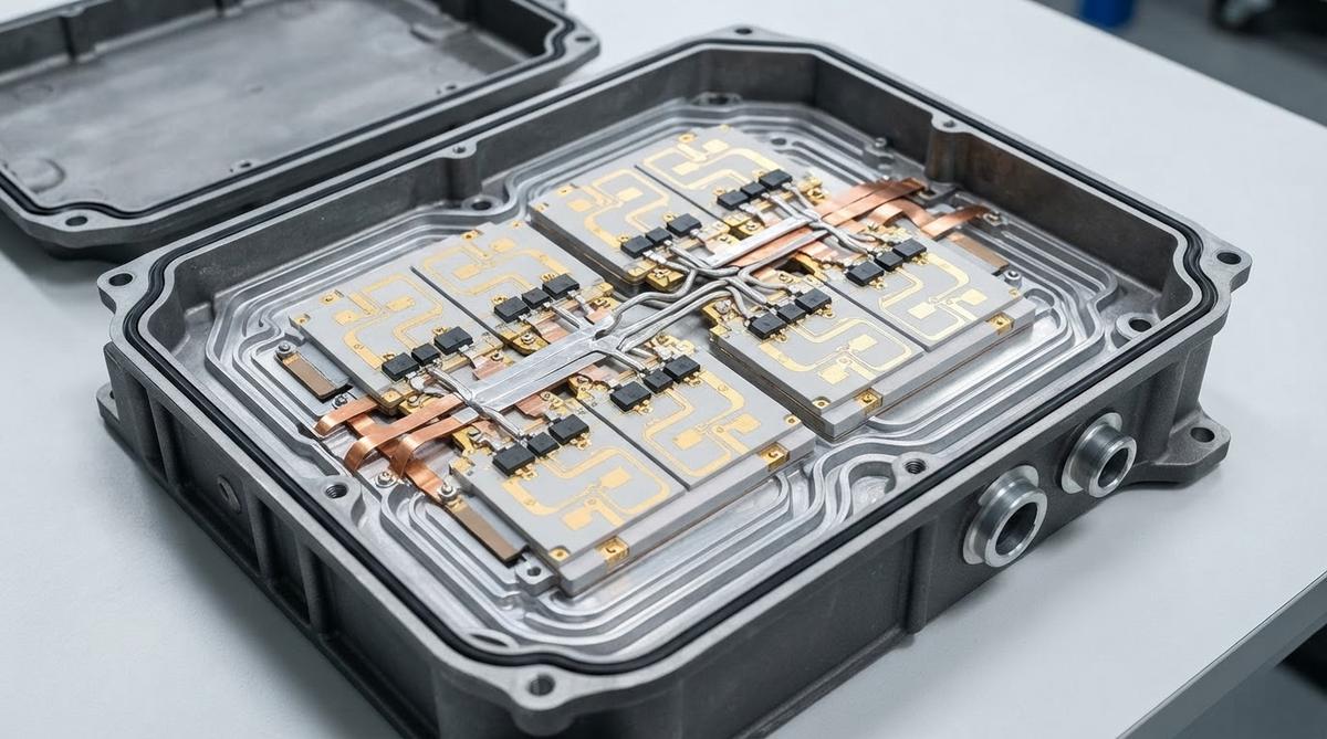
The shift from silicon IGBTs to SiC MOSFETs in 800 V EV platforms (Hyundai E-GMP, Porsche PPE, GM Ultium) pushes junction temperatures from 150 °C toward 175–200 °C. SiC also switches faster (50–100 kHz vs. 10–20 kHz for IGBTs), generating sharper thermal transients. AlN handles both demands: its thermal conductivity barely degrades up to 300 °C, and its mechanical strength is sufficient at 175 °C continuous. For a focused comparison of AlN in SiC module designs, see AlN substrates for SiC power modules.
DBC vs. AMB Metallization on AlN for EV Use
Both DBC and AMB bond copper foil to the AlN ceramic, but through different mechanisms. DBC uses a Cu-O eutectic at ~1,065 °C; AMB uses a reactive braze alloy (typically TiCuAg) at ~850 °C. In an EV power module AlN PCB, the choice matters for two reasons:
- Copper thickness: DBC on AlN is typically limited to 0.3 mm Cu. AMB supports 0.8 mm or thicker, which reduces I²R losses in 200+ A bus bars.
- Thermal cycling reliability: AMB’s braze layer absorbs more strain than DBC’s oxide bond, giving 2–3× longer cycle life under –55 °C / +150 °C swings (per Infineon AN2019-03 application note on power module substrates).
AMB costs 20–40% more than DBC for the same substrate size. If your module operates below 100 A and cycles are moderate (e.g., an auxiliary inverter), DBC on AlN is often sufficient. For main traction inverters, AMB is the industry standard. Custom AlN substrates are available in both metallization types through AlN custom fabrication.
When Not to Use AlN for EV Power Modules
AlN is not always the right answer, even in automotive applications:
- Low power density (<50 W/cm²): 96% alumina DBC costs 3–5× less and handles the thermal load. Auxiliary converters, on-board chargers below 7 kW, and DC-DC converters under 3 kW rarely need AlN.
- Extreme mechanical shock: Si₃N₄ (silicon nitride) offers 2–3× the fracture toughness of AlN (6–8 MPa·√m vs. 2.5–3.5 MPa·√m). For modules mounted directly on the motor housing where vibration exceeds 30 g, Si₃N₄ AMB may be more reliable.
- Cost-driven designs: If the thermal budget can be closed with an aluminum MCPCB and a larger heatsink, the cost saving is substantial. An EV power module AlN PCB is justified when size, weight, or junction temperature constraints cannot be met any other way.
FAQ
Can AlN substrates handle 800 V battery bus voltages?
Yes. AlN has a dielectric strength of 15–17 kV/mm (per IEC 60672 at 25 °C). A 0.635 mm substrate withstands roughly 9.5–10.8 kV DC, far exceeding the 800 V bus plus required isolation margins defined in IEC 60664-1.
Does AlN degrade when exposed to humidity?
Unprotected AlN hydrolyzes slowly in the presence of moisture, forming aluminum hydroxide on the surface. In a sealed power module with conformal coating or encapsulation, this is not a practical concern. For bare substrates stored in warehouse conditions, keep relative humidity below 60% and use vacuum-sealed packaging.
What surface finishes work on AlN DBC for EV modules?
Electroless nickel / immersion gold (ENIG) is the most common finish for soldering SiC die to AlN DBC. Ni/Au plating (electrolytic) is used when wire bonding is required. Silver sintering—increasingly adopted for SiC die attach—requires a bare copper or thin Ag-plated surface. See available options on the surface finishes overview.
How does AlN compare to Si₃N₄ for traction inverters?
Si₃N₄ has roughly 3× the fracture toughness but only 40–90 W/mK thermal conductivity. For the highest power densities, AlN wins on thermal performance. For applications with extreme vibration or very thick copper (≥0.5 mm), Si₃N₄ AMB offers better mechanical reliability. Many Tier 1 suppliers use Si₃N₄ for main inverters and AlN for auxiliary modules.
What is the typical lead time for AlN DBC substrates in automotive volumes?
Prototype quantities (10–50 pieces) typically ship in 3–5 weeks. Production volumes (1,000+ per month) require 8–14 weeks depending on metallization, patterning complexity, and surface finish. Planning 16 weeks of lead time for initial PPAP runs is prudent.
Next Step
If your traction inverter design needs an EV power module AlN PCB, start by defining the die size, power dissipation, and target thermal resistance. Our engineers can review your thermal stack and recommend a substrate thickness, metallization type, and layout matched to your module geometry. For industrial power supply modules that share similar requirements at lower voltages, see AlN PCBs for industrial power supplies.