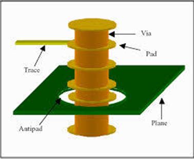
What is a PCB Antipad?
A PCB (printed circuit board) antipad, also known as a thermal relief or thermal pad, is a design feature used to improve solderability and reduce thermal stress on plated through holes (PTHs). An antipad is essentially a clearance area around a PTH where the copper plane or pour is pulled back, creating a “spoke-like” pattern of copper connecting the pad to the surrounding plane.
The primary purpose of an antipad is to limit the amount of heat that is conducted away from the PTH during the soldering process. Without an antipad, the large copper area surrounding the PTH would act as a heat sink, making it difficult for the solder to properly flow and form a strong connection. By reducing the copper area in direct contact with the PTH, the antipad allows the hole to reach the necessary temperature for effective soldering.
Benefits of Using Antipads
1. Improved Solderability
One of the main advantages of using antipads in PCB design is enhanced solderability. By reducing the thermal mass around the PTH, the antipad allows the hole to reach the required temperature for proper solder flow. This results in stronger, more reliable solder joints and reduces the risk of cold or weak connections.
2. Reduced Thermal Stress
Antipads also help to minimize thermal stress on the PTH during the soldering process. When a large copper area is in direct contact with the PTH, it can cause uneven heating and cooling, leading to mechanical stress on the hole. This stress can result in cracking or delamination of the plated copper, compromising the integrity of the connection. By limiting the copper area around the PTH, antipads promote more uniform heating and cooling, reducing thermal stress and improving the long-term reliability of the solder joint.
3. Better Solder Wicking
Another benefit of using antipads is improved solder wicking. Wicking refers to the ability of molten solder to flow up the PTH and form a strong connection with the component lead. When a large copper area surrounds the PTH, it can hinder the wicking process by drawing heat away from the hole too quickly. Antipads help to concentrate the heat at the PTH, promoting better solder wicking and ensuring a more reliable connection.

Designing Antipads
When designing antipads for your PCB, there are several factors to consider, including the size of the PTH, the thickness of the PCB, and the thermal requirements of the components being used.
Antipad Size
The size of the antipad is typically expressed as a ratio of the PTH diameter to the antipad diameter. A common ratio is 2:1, meaning the antipad diameter is twice the size of the PTH diameter. For example, if the PTH has a diameter of 0.5mm, the antipad would have a diameter of 1mm.
However, the optimal antipad size can vary depending on the specific requirements of your design. In some cases, a larger antipad may be necessary to provide sufficient thermal relief, while in others, a smaller antipad may be preferable to maintain signal integrity or to conserve board space.
Spoke Width
The width of the copper spokes connecting the PTH to the surrounding plane is another important consideration when designing antipads. Wider spokes provide a lower resistance path for heat to dissipate, while narrower spokes can help to concentrate the heat at the PTH for better soldering.
A common spoke width is 0.25mm, but this can be adjusted based on the thermal requirements of your design. It’s important to strike a balance between providing adequate thermal relief and maintaining sufficient copper for reliable electrical connections.
Thermal Pad Size
In some cases, it may be necessary to use a larger copper pad around the PTH to provide additional Thermal dissipation. This is particularly true for high-power components or those that generate significant amounts of heat. The size of the thermal pad should be carefully considered to ensure it provides sufficient heat sinking without compromising signal integrity or board space.

Antipad Design Guidelines
When designing antipads for your PCB, there are several best practices to keep in mind:
-
Use a consistent antipad size and shape throughout your design to ensure uniform soldering and thermal relief.
-
Avoid placing antipads too close to other copper features, such as traces or planes, to prevent shorting or signal integrity issues.
-
Consider the thermal requirements of your components when selecting antipad sizes and spoke widths.
-
Use thermal simulation tools to validate your antipad design and ensure it provides adequate thermal relief.
-
Follow the manufacturer’s recommendations for antipad design when using specialized components or materials.

Antipad vs. No Antipad
While antipads offer several benefits for PCB design, there are some situations where they may not be necessary or desirable. In general, antipads are most beneficial for PTHs that will be soldered, as they help to ensure strong, reliable connections. However, for PTHs that will not be soldered, such as those used for mechanical support or alignment, antipads may not provide any significant advantage.
Additionally, in some high-speed or high-frequency designs, antipads can actually degrade signal integrity by creating discontinuities in the ground plane. In these cases, it may be preferable to use a solid copper pour around the PTH to maintain a consistent reference plane.
Ultimately, the decision to use antipads or not will depend on the specific requirements of your design, including the thermal demands of your components, the signal integrity constraints of your circuit, and the manufacturing processes being used.
FAQ
1. What is the purpose of an antipad in PCB design?
The primary purpose of an antipad is to provide thermal relief for plated through holes (PTHs) during the soldering process. By reducing the copper area in direct contact with the PTH, the antipad allows the hole to reach the necessary temperature for effective soldering, resulting in stronger, more reliable connections.
2. How do I determine the appropriate antipad size for my design?
The size of the antipad is typically expressed as a ratio of the PTH diameter to the antipad diameter. A common ratio is 2:1, meaning the antipad diameter is twice the size of the PTH diameter. However, the optimal antipad size can vary depending on the specific thermal and electrical requirements of your design. It’s important to consider factors such as the thickness of the PCB, the power dissipation of the components, and the signal integrity constraints of your circuit when selecting an antipad size.
3. Can antipads be used for surface mount components?
Antipads are primarily used for through-hole components, as they provide thermal relief for plated through holes during the soldering process. Surface mount components do not require antipads, as they are soldered directly to the surface of the PCB and do not rely on PTHs for electrical and mechanical connection. However, surface mount pads may still benefit from thermal relief designs, such as thermal spokes or Thermal Pads, to improve heat dissipation and prevent solder joint failures.
4. Are there any situations where antipads should not be used?
While antipads offer several benefits for PCB design, there are some situations where they may not be necessary or desirable. For PTHs that will not be soldered, such as those used for mechanical support or alignment, antipads may not provide any significant advantage. Additionally, in some high-speed or high-frequency designs, antipads can actually degrade signal integrity by creating discontinuities in the ground plane. In these cases, it may be preferable to use a solid copper pour around the PTH to maintain a consistent reference plane.
5. How do I ensure my antipad design is effective?
To ensure your antipad design is effective, it’s important to follow best practices and guidelines, such as using a consistent antipad size and shape throughout your design, avoiding placing antipads too close to other copper features, and considering the thermal requirements of your components when selecting antipad sizes and spoke widths. Additionally, using thermal simulation tools can help validate your antipad design and ensure it provides adequate thermal relief. Finally, it’s important to follow the manufacturer’s recommendations for antipad design when using specialized components or materials.
Conclusion
Antipads are a valuable tool for improving solderability, reducing thermal stress, and ensuring reliable connections in PCB design. By providing thermal relief for plated through holes, antipads help to concentrate heat at the PTH during the soldering process, promoting better solder flow and stronger joints.
When designing antipads, it’s important to consider factors such as the size of the PTH, the thickness of the PCB, and the thermal requirements of the components being used. By following best practices and guidelines, such as using a consistent antipad size and shape, avoiding placing antipads too close to other copper features, and considering the thermal requirements of your components, you can ensure your antipad design is effective and reliable.
While antipads offer several benefits, there are some situations where they may not be necessary or desirable, such as for PTHs that will not be soldered or in high-speed designs where signal integrity is a concern. Ultimately, the decision to use antipads or not will depend on the specific requirements of your design.
By understanding the principles and best practices of antipad design, you can create PCBs that are more reliable, efficient, and cost-effective. Whether you are a seasoned PCB designer or just starting out, taking the time to properly design and implement antipads can help ensure the success of your projects.
| Antipad Design Guidelines | Explanation |
|---|---|
| Use a consistent antipad size and shape | Ensures uniform soldering and thermal relief throughout the design |
| Avoid placing antipads too close to other copper | Prevents shorting or signal integrity issues |
| Consider thermal requirements when selecting size | Ensures sufficient thermal relief for components |
| Use thermal simulation tools for validation | Helps validate the antipad design and ensure adequate thermal relief |
| Follow manufacturer’s recommendations | Ensures proper antipad design when using specialized components or materials |
By following these guidelines and understanding the principles behind antipad design, you can create PCBs that are reliable, efficient, and cost-effective. Whether you are working on a simple prototype or a complex, high-density design, properly implementing antipads can help ensure the success of your project.


Leave a Reply