Ceramic PCB warpage occurs when unequal stress across the substrate forces it to bow or twist out of plane. The most common driver is CTE mismatch between the ceramic body and the metallisation layers, but firing profiles, copper distribution, and panel geometry all play a role. On a well-designed ceramic board, total warpage stays below 0.5 % of the diagonal per IPC-TM-650, Method 2.4.22. Exceeding that threshold causes solder-joint opens, die-attach voids, and assembly rejects.
Key Takeaways
- IPC-TM-650 Method 2.4.22 defines the standard measurement for bow and twist; most ceramic assemblies target ≤ 0.5 % of the board diagonal.
- CTE mismatch between copper (≈ 17 ppm/°C) and alumina (≈ 7 ppm/°C at 25–300 °C) is the primary warpage driver in DBC and DPC substrates.
- Symmetric copper balance — matching copper area and thickness on top and bottom — is the single most effective design-stage countermeasure.
- Thicker substrates resist bending but add thermal resistance; 0.635 mm Al₂O₃ warps roughly half as much as 0.38 mm under the same copper load.
- Post-fire lapping can recover flatness to ≤ 25 µm across a 50 × 50 mm panel, but adds cost and lead time.
What Causes Warpage in Ceramic PCBs?
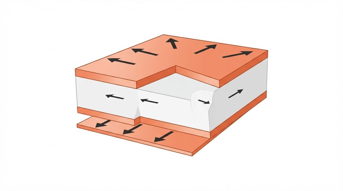
Warpage is a strain problem. Any time one face of the substrate expands or contracts more than the other, the board curves. In organic PCBs the culprit is usually resin cure shrinkage. In ceramics, three mechanisms dominate.
CTE Mismatch Between Ceramic and Metal
Copper’s CTE is roughly 17 ppm/°C. Alumina 96 % sits near 7.1 ppm/°C (25–300 °C, per CoorsTek ADS-96R datasheet). Aluminum nitride is lower still at about 4.5 ppm/°C. When a DBC or thick-film board cools from bonding or firing temperature, the copper wants to shrink more than the ceramic. If the copper is only on one side, the board bows toward the copper. The magnitude scales with ΔT, the copper-to-ceramic thickness ratio, and the area of copper coverage.
For boards operating across wide temperature swings — such as those designed for PCB survival above 200 °C — the accumulated thermal strain is larger, and warpage control becomes even more critical.
Asymmetric Copper Distribution
Even when both sides carry copper, an imbalance in coverage area or pattern density creates a net bending moment. A top layer with 80 % copper fill and a bottom layer with 30 % fill will warp predictably toward the heavier side on cooling. This is the same copper-balance problem familiar from FR-4 design, but the consequences are worse because ceramic is brittle — a warped alumina substrate that flexes during handling can crack.
Firing and Bonding Stresses
HTCC substrates are co-fired at 1 500–1 600 °C. LTCC fires at 850–900 °C. DBC bonds copper at roughly 1 065 °C in a nitrogen atmosphere. Non-uniform temperature distribution inside the furnace, or a too-fast cooling ramp, locks in residual stress gradients that manifest as warpage at room temperature. Multi-zone furnaces with controlled ramp rates (typically 2–5 °C/min cooling through the 600–200 °C range) reduce this effect.
IPC Flatness Limits for Ceramic Substrates
IPC-TM-650, Method 2.4.22 defines bow (cylindrical curvature) and twist (helical deformation) as percentages of the board’s longest diagonal. The table below shows typical acceptance limits.
| Parameter | Limit | Unit | Condition | Source |
|---|---|---|---|---|
| Bow | ≤ 0.50 | % of diagonal | Room temp, unloaded | IPC-TM-650, 2.4.22 |
| Twist | ≤ 0.50 | % of diagonal | Room temp, unloaded | IPC-TM-650, 2.4.22 |
| Local flatness (die-attach pad) | ≤ 25 | µm over 10 × 10 mm | After lapping | Typical power-module spec |
| Surface roughness (Ra) | 0.3–0.8 | µm | As-fired Al₂O₃ 96 % | CoorsTek ADS-96R datasheet |
Typical values for commercially available material, for comparison only. Confirm against the datasheet for your specific grade.
For die-attach applications in IGBT or SiC power modules, OEMs often tighten the local flatness spec to ≤ 15 µm over the die footprint. Meeting that on a substrate larger than about 40 × 40 mm usually requires post-fire lapping.
Worked Example: Estimating Bow from CTE Mismatch
A simplified Timoshenko bi-metal strip model gives a first-order estimate of curvature radius ρ for a ceramic-copper bilayer. For a 0.635 mm Al₂O₃ substrate with 0.3 mm DBC copper on one side only, cooling from 1 065 °C to 25 °C:
- ΔT = 1 040 °C
- Δα = (17.0 − 7.1) × 10⁻⁶ = 9.9 × 10⁻⁶ /°C
- Total thickness h = 0.935 mm
- Thickness ratio m = 0.3 / 0.635 ≈ 0.47
- Modulus ratio n = E_Cu / E_Al₂O₃ ≈ 120 / 370 ≈ 0.32
Plugging into the Timoshenko formula, the radius of curvature comes out near 120–150 mm — which on a 50 mm-long substrate gives a centre deflection of roughly 2–2.5 mm, or about 3–4 % of the diagonal. That is far outside spec. This is exactly why single-sided DBC without a balancing copper layer on the back is rarely used for anything wider than about 25 mm.
Adding a matching copper layer on the bottom — even an unpatterned ground plane — brings the net bending moment close to zero and drops bow to well under 0.5 %. This is the core principle of copper balance.
How to Control Ceramic PCB Warpage
1. Design Symmetric Copper Balance
Match the copper area fraction on top and bottom to within 10–15 %. Where the signal layer is sparse, add copper thieving (non-functional copper fill) on the opposite side. For multilayer ceramic PCB builds, balance each pair of layers about the neutral axis, just as you would in a multilayer FR-4 stackup.
Enter your top-side and bottom-side copper coverage to check whether your layout is balanced and estimate the resulting warpage tendency:
[pcb_calc type=”copper-balance”]
2. Choose the Right Substrate Thickness
Stiffness scales with the cube of thickness. A 0.635 mm alumina substrate is roughly 4.6× stiffer in bending than a 0.38 mm one. If your thermal budget allows the extra thickness — thermal resistance through the substrate scales linearly — use it.
3. Specify Material Wisely
AlN (CTE ≈ 4.5 ppm/°C) has a larger CTE gap to copper than Al₂O₃ (CTE ≈ 7.1 ppm/°C), so AlN boards are more warpage-sensitive for the same copper configuration. Si₃N₄ (CTE ≈ 3.2 ppm/°C) has the widest gap but also the highest fracture toughness (6–7 MPa·√m), so it tolerates residual stress better without cracking. See the full ceramic substrate material comparison for property data.
4. Control Firing and Cooling Profiles
Slow, uniform cooling through the high-stress temperature window (roughly 800 °C down to 200 °C) lets residual stresses relax. A cooling rate above 10 °C/min in this range measurably increases warpage in DBC panels larger than 100 × 100 mm. Multi-zone tunnel kilns with independent heater control outperform batch furnaces for flatness consistency.
5. Post-Process Flattening
Lapping (surface grinding with diamond slurry) can bring a warped panel back to ≤ 25 µm flatness. It removes 10–50 µm of material per pass. For panels that only need moderate correction, a weighted anneal — holding the panel flat under a graphite weight at 400–500 °C for 30–60 min — can relieve residual stress without material removal.
When Warpage Is Not the Real Problem
If your substrate is small (under 15 × 15 mm) and carries copper on both sides, warpage is unlikely to exceed spec regardless of material choice. In that case, spend your engineering effort on simulating thermal performance rather than optimising flatness.
For large-area, single-sided metallisation where flatness is non-negotiable, consider an aluminium-core MCPCB or a copper baseplate with a bonded ceramic insulator. These composite structures use the metal’s stiffness to enforce flatness, trading some dielectric performance for mechanical stability. Ceramic is not always the right substrate when the dominant requirement is flatness over a large area at low cost.
Frequently Asked Questions
How flat should a ceramic PCB be for SMD assembly?
Most SMD reflow processes require bow and twist below 0.5 % of the board diagonal, per IPC-TM-650 Method 2.4.22. For fine-pitch BGA (≤ 0.5 mm pitch), tighter limits of 0.3 % or even 0.2 % may be needed to avoid solder bridging or opens.
Does warpage get worse after reflow soldering?
Yes. A board that is flat at room temperature can warp during reflow as the copper and ceramic expand at different rates. Peak reflow at 260 °C adds roughly 250 °C of ΔT beyond room temperature, generating additional transient bow. The board usually returns close to its original shape on cooling, but any pre-existing asymmetry amplifies the peak deflection.
Can I fix warpage by adding copper thieving after layout is done?
Copper thieving on the lighter side is the standard fix. Add non-functional copper pads or fills to bring the coverage within 10–15 % of the opposite side. Keep thieving pads away from RF signal traces to avoid parasitic capacitance, and connect them to ground or leave them floating depending on your EMC strategy.
Is AlN more prone to warpage than alumina?
AlN’s CTE (≈ 4.5 ppm/°C) is further from copper’s CTE (≈ 17 ppm/°C) than alumina’s (≈ 7.1 ppm/°C), so the mismatch strain is about 25 % larger for the same ΔT. In practice, AlN DBC panels require tighter copper-balance tolerances and slower cooling profiles to meet the same flatness spec.
What measurement method should I specify for incoming inspection?
Specify IPC-TM-650, Method 2.4.22 for bow and twist. For local flatness over a die-attach pad, a non-contact optical profilometer (white-light interferometry) with a measurement area matching the pad footprint gives repeatable results to ± 1 µm. Avoid dial indicators on bare ceramic — point loading can chip the edge.
Next Step
If you have a layout in progress and want to check whether your copper distribution will meet flatness targets, use the copper-balance tool above or upload your Gerber files for a design review. For questions about substrate thickness, material selection, or post-processing options, browse the ceramic PCB FAQ or request a quote directly.