Ceramic PCB thermal management works by conducting heat directly through the substrate rather than relying on vias or metal-core insulation layers to work around a thermally resistive dielectric. A 96% alumina (Al₂O₃) substrate conducts heat at 24–28 W/m·K, aluminum nitride (AlN) at 170–200 W/m·K, and silicon nitride (Si₃N₄) at 70–90 W/m·K—compared to 0.3–0.4 W/m·K for standard FR-4. That difference, two to three orders of magnitude, is what makes ceramic PCB thermal management the default choice for power electronics, high-brightness LEDs, and RF amplifiers where junction temperature directly limits reliability.
Key Takeaways
- AlN substrates offer 170–200 W/m·K thermal conductivity, roughly 6–8× that of 96% alumina and 500× that of FR-4 (per Kyocera and Maruwa datasheets).
- Replacing a 1.0 mm FR-4 dielectric with 0.635 mm 96% alumina under a 10 W source cuts substrate thermal resistance from ~83 °C/W to ~0.23 °C/W—a reduction of over 99%.
- CTE mismatch between ceramic and copper or solder is the primary mechanical risk; Si₃N₄ tolerates this stress best due to fracture toughness of 6–7 MPa·m½.
- Ceramic is not cost-effective for boards dissipating under 1–2 W where standard FR-4 or metal-core PCB (MCPCB) already keeps junctions within spec.
- Thermal simulation before layout commit prevents over-specifying material—AlN where alumina would suffice wastes 3–5× the substrate cost.
Why Ceramic PCB Thermal Management Outperforms Organic Dielectrics
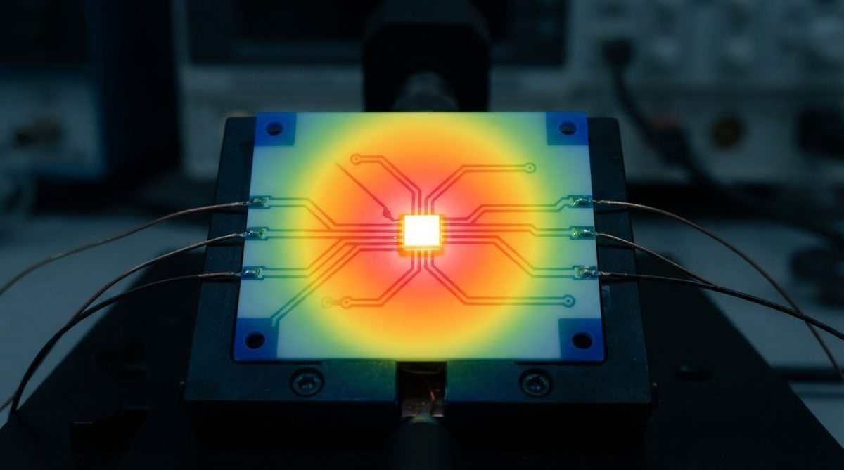
In an FR-4 stack-up, the glass-epoxy dielectric acts as a thermal insulator. Heat must travel through copper planes and plated vias to reach the opposite side. Even with a dense via field, effective through-board conductivity rarely exceeds 2–4 W/m·K. Metal-core PCBs improve this with an aluminum base, but the thin dielectric layer between copper and core (typically 75–100 µm of thermally filled prepreg at 1–3 W/m·K) remains the bottleneck.
A ceramic substrate eliminates that bottleneck. The dielectric is the heat path. With AlN at 170–200 W/m·K, the substrate conducts heat nearly as well as aluminum metal (205 W/m·K) while providing full electrical isolation rated to 15–20 kV/mm. This lets you mount bare die directly on the ceramic surface, solder power devices with minimal thermal interface layers, and still maintain dielectric withstand voltages that organic boards cannot match at the same thickness.
Ceramic Substrate Thermal Properties Compared
| Parameter | 96% Al₂O₃ | 99.6% Al₂O₃ | AlN | Si₃N₄ | FR-4 (ref.) |
|---|---|---|---|---|---|
| Thermal conductivity (W/m·K, 20 °C) | 24–28 | 28–33 | 170–200 | 70–90 | 0.3–0.4 |
| CTE (ppm/°C, 25–400 °C) | 7.0–7.4 | 7.2–7.6 | 4.4–4.7 | 2.5–3.4 | 14–17 |
| Dielectric strength (kV/mm) | 10–15 | 12–17 | 15–20 | 12–16 | 20–40 |
| Max continuous use temp (°C) | ~1 000 | ~1 000 | ~800 (oxidation onset) | ~1 000 | 130–180 |
| Flexural strength (MPa, ASTM C1161) | 300–380 | 350–400 | 300–350 | 650–800 | 400–550 |
| Fracture toughness (MPa·m½) | 3.5–4.0 | 3.5–4.2 | 2.5–3.0 | 6.0–7.0 | N/A |
Typical values for commercially available material, for comparison only. Confirm against the datasheet for your specific grade. Sources: Kyocera fine ceramics catalog (2023), Maruwa AlN datasheet, CoorsTek technical data.
The table shows a clear hierarchy for raw thermal conductivity: AlN > Si₃N₄ > Al₂O₃. But thermal conductivity alone does not determine which material you should buy. CTE match to silicon (2.6 ppm/°C) and GaN (3.2 ppm/°C) matters for die-attach reliability, and Si₃N₄ thermal properties make it the strongest choice for power modules that undergo aggressive thermal cycling. For a full breakdown of each substrate option, see the ceramic PCB material comparison.
Worked Example: Thermal Resistance Through a Ceramic Substrate
Effective ceramic PCB thermal management starts with calculating the substrate’s contribution to total thermal resistance. The one-dimensional formula is:
Rth = t / (k × A)
where t = substrate thickness (m), k = thermal conductivity (W/m·K), and A = heat-spreading area (m²).
Scenario: 10 W GaN HEMT, 3 mm × 3 mm die pad
Assume the die sits on a 0.635 mm (25 mil) substrate. The heat-spreading area at the die interface is approximately 3 × 3 mm = 9 × 10⁻⁶ m².
| Substrate | k (W/m·K) | Rth, substrate (°C/W) | ΔT at 10 W (°C) |
|---|---|---|---|
| FR-4 | 0.35 | 201.6 | 2 016 |
| 96% Al₂O₃ | 26 | 2.72 | 27.2 |
| AlN | 180 | 0.39 | 3.9 |
| Si₃N₄ | 80 | 0.88 | 8.8 |
1-D conduction only, no spreading. Real spreading into a larger board area reduces effective Rth further.
The FR-4 number is obviously unworkable—the die would destroy itself instantly. Even with a dense thermal via array in FR-4, you might bring that down to 30–50 °C/W, still far above what alumina achieves with zero vias. For a deeper walkthrough of the math, including spreading resistance and interface layers, see how to calculate thermal resistance of a ceramic PCB.
Enter your own substrate area, thickness, and dissipated power below to estimate junction temperature rise for your specific design.
Choosing the Right Ceramic for Your Thermal Budget
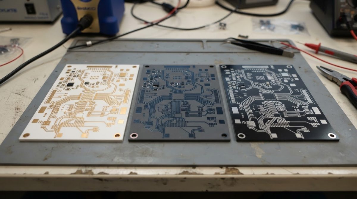
Start from your thermal budget, not from the material catalog. Work backward: determine the maximum allowable junction temperature (from the device datasheet), subtract worst-case ambient, then allocate thermal resistance across each layer—die attach, substrate, TIM, heatsink. The substrate Rth tells you which ceramic grade your ceramic PCB thermal management strategy actually requires.
When 96% alumina is enough
For power densities below roughly 30–50 W/cm², 96% Al₂O₃ at 0.38–1.0 mm thickness keeps substrate ΔT under 15–25 °C. This covers most LED arrays, sensor substrates, and medium-power DC-DC converters. Alumina is the lowest-cost ceramic option, widely available, and compatible with DBC, DPC, thick-film, and thin-film metallization.
When you need AlN
Above 50 W/cm², or when die-attach CTE match to GaN or SiC is critical, AlN becomes necessary. Its 4.4–4.7 ppm/°C CTE closely matches SiC (4.0 ppm/°C), reducing solder joint fatigue under thermal cycling. AlN costs 3–5× more than alumina per unit area, and it requires nitrogen-atmosphere sintering, so lead times tend to run longer. For boards operating in extreme environments, review what temperature ceramic PCBs can handle.
When Si₃N₄ wins
In traction inverters, EV power modules, and other applications with thousands of deep thermal cycles (ΔT > 100 °C per cycle), Si₃N₄’s fracture toughness (6–7 MPa·m½) prevents substrate cracking that would kill an AlN board. Its thermal conductivity (70–90 W/m·K) is lower than AlN, but the mechanical reliability over a 15-year vehicle life makes the trade-off worthwhile. AMB (active metal brazing) is the standard metallization process for Si₃N₄ power substrates.
Design Rules That Improve Ceramic PCB Thermal Management
Material selection accounts for perhaps 60% of thermal performance. The remaining 40% comes from layout and construction decisions.
- Minimize substrate thickness. Rth scales linearly with thickness. Going from 1.0 mm to 0.38 mm alumina cuts substrate resistance by 62%. The trade-off is mechanical strength and warpage control during metallization.
- Maximize heat-spreading area. Extend the ground or thermal pad copper beyond the die footprint. A copper plane 2–3× the die area on both sides of the substrate allows lateral spreading before heat enters the heatsink.
- Use thermal vias where geometry allows. Even in ceramic, filled copper vias under a die pad reduce local Rth by 10–30%, depending on via density and fill quality. See thermal via design for ceramic substrates for spacing and diameter guidelines.
- Control die-attach void fraction. Solder voids under the die act as thermal insulators. X-ray inspection should verify void fraction below 5% for power devices, per MIL-STD-883 Method 2030.
- Simulate before committing. A 2-hour FEA run can confirm whether 96% alumina meets your thermal budget or whether you genuinely need AlN. Run thermal simulation on your ceramic board with realistic boundary conditions—forced convection coefficients, not just fixed-temperature heatsink assumptions.
When NOT to Use Ceramic for Thermal Management
Ceramic substrates are not always the right answer. Consider alternatives in these situations:
- Total dissipation under 1–2 W with no high-density hotspots. Standard FR-4 with a copper pour and a few thermal vias handles this at a fraction of the cost.
- Board area larger than ~150 mm × 150 mm with moderate power density. Metal-core PCBs (aluminum or copper base, 1–3 W/m·K dielectric) offer better cost per cm² and are available in larger panels. Ceramic substrates are typically limited to panels under 150 mm × 150 mm.
- Designs needing >6 layers of signal routing. Multilayer ceramic builds (HTCC, LTCC) exist but are expensive and limited in layer count compared to organic stack-ups. If your thermal problem is localized, a hybrid approach—ceramic substrate for the power section, FR-4 for the control section—often wins.
- Cost-sensitive consumer products. Ceramic substrate pricing starts at roughly 5–10× the cost of equivalent FR-4 area. If the product’s bill of materials cannot absorb that, redesigning for lower power density on an organic board may be more practical.
Frequently Asked Questions
Can I solder standard SMD components onto a ceramic PCB?
Yes. Ceramic PCBs with DPC or DBC metallization accept standard reflow soldering with SAC305 or other lead-free alloys. The key difference is that ceramic’s lower CTE (4.4–7.4 ppm/°C vs. 14–17 for FR-4) creates higher shear stress on large solder joints during thermal cycling, so you may need to adjust pad geometry or use compliant underfill for BGAs larger than about 15 mm.
Does ceramic PCB thermal conductivity degrade at high temperatures?
It decreases, but remains far above organic alternatives. AlN thermal conductivity drops from ~180 W/m·K at 25 °C to ~120 W/m·K at 300 °C (per Kyocera data). Alumina drops from ~26 W/m·K to ~15 W/m·K over the same range. Factor this derating into your ceramic PCB thermal management budget if the substrate will operate above 150 °C continuously.
How does ceramic compare to insulated metal substrate (IMS) for LED thermal management?
IMS boards use a thin dielectric layer (50–100 µm) over an aluminum base, achieving effective through-thickness conductivity of 1–3 W/m·K. A 0.635 mm alumina substrate at 26 W/m·K delivers lower substrate Rth and much higher dielectric withstand voltage. For single LEDs under 3 W, IMS is cheaper and adequate. For arrays above 10 W or for UV LEDs requiring hermetic packaging, ceramic is the better path.
What is the thinnest ceramic substrate available for thermal management?
Production substrates are commonly available down to 0.25 mm (250 µm) in alumina and AlN. Thinner substrates (100–150 µm) exist but are fragile and require careful handling during assembly. Thinner substrates reduce Rth proportionally but increase warpage risk during metallization and reflow.
Do I need a heatsink on the back of a ceramic PCB?
Usually, yes. The ceramic substrate conducts heat efficiently to its back surface, but it does not dissipate that heat to air on its own—its surface area is too small for meaningful convection. Attach a heatsink, bond the board to a chassis, or design forced airflow across the back surface. The ceramic’s job is to get heat from the die to the heatsink interface with minimal ΔT; the heatsink’s job is to reject it to ambient.