96% alumina (Al2O3) substrates offer thermal conductivity of 24–28 W/m·K at 25 °C—roughly 100× better than standard FR-4 (0.25–0.3 W/m·K) and adequate for most power-dissipation needs below about 50 W/cm². This alumina 96% Al2O3 thermal design guide gives you the numbers, layout rules, and worked calculations to decide whether 96% alumina handles your thermal budget or whether you need to step up to a costlier material.
Key Takeaways
- 96% alumina conducts 24–28 W/m·K at 25 °C, dropping to roughly 15–18 W/m·K at 300 °C (per Kyocera A-493 datasheet).
- Thermal resistance through a 0.635 mm alumina substrate under a 5 × 5 mm die is approximately 0.98 °C/W—workable for many power devices under 10 W.
- The substrate itself survives above 1 000 °C, but copper metallisation and solder joints set practical limits near 300–400 °C depending on attach method.
- For heat fluxes above ~80 W/cm², aluminum nitride (170–200 W/m·K) or a ceramic heat spreader design becomes necessary.
- 96% alumina is the lowest-cost ceramic substrate option, typically 30–50 % cheaper per unit area than AlN.
Alumina 96% Al2O3 Thermal Design: Property Data at a Glance
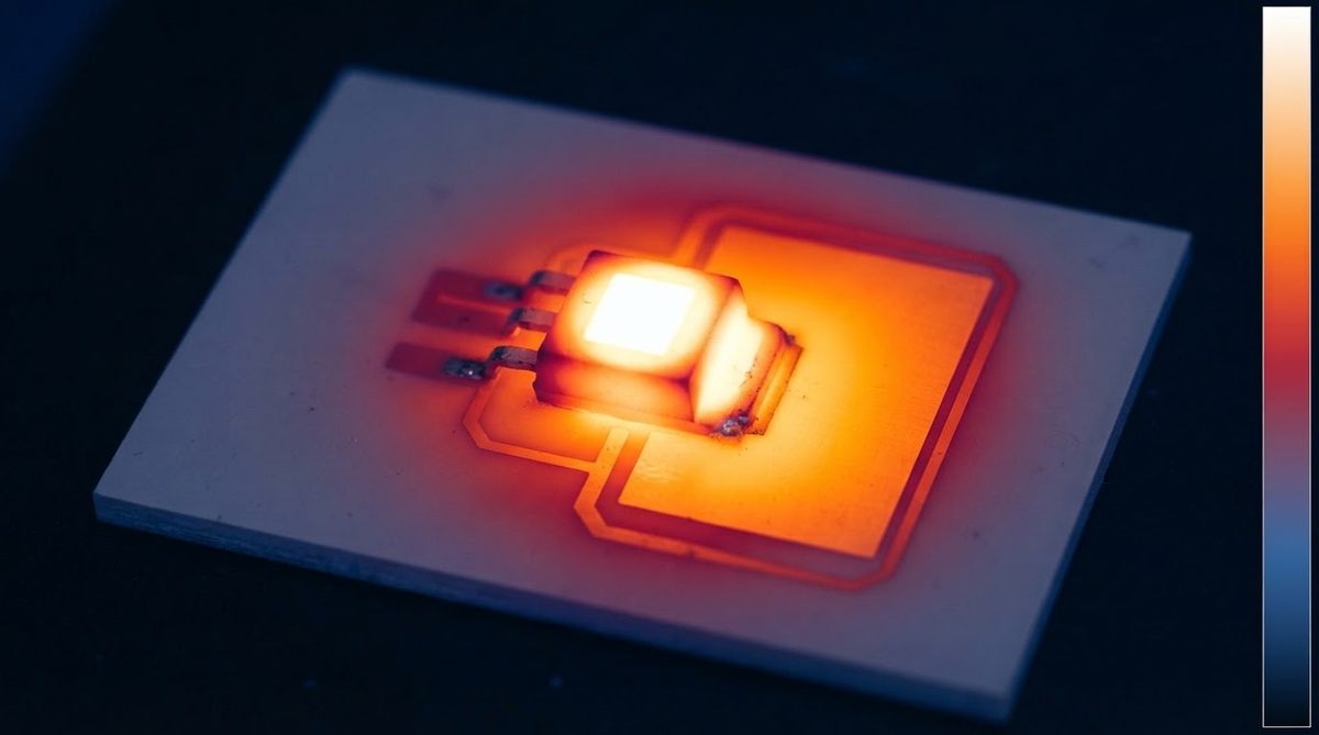
| Parameter | Value | Unit | Condition | Source |
|---|---|---|---|---|
| Thermal conductivity | 24–28 | W/m·K | 25 °C, ASTM E1461 | Kyocera A-493, CoorsTek ADS-96R |
| Thermal conductivity | 15–18 | W/m·K | 300 °C | Kyocera A-493 |
| CTE | 6.5–7.2 | ppm/°C | 25–300 °C | CoorsTek ADS-96R |
| Specific heat | 780–800 | J/kg·K | 25 °C | CeramTec Rubalit 708S |
| Density | 3.72–3.78 | g/cm³ | — | Kyocera A-493 |
| Max. continuous use temp. (substrate only) | 1 600 | °C | No metallisation | CoorsTek ADS-96R |
| Dielectric strength | 14–16 | kV/mm | AC, 60 Hz, ASTM D149 | CoorsTek ADS-96R |
Typical values for commercially available material, for comparison only. Confirm against the datasheet for your specific grade.
Worked Example: Thermal Resistance Through a 96% Alumina Substrate
Suppose you mount a 5 × 5 mm power MOSFET dissipating 8 W on a 0.635 mm thick 96% alumina substrate. The one-dimensional conduction resistance through the ceramic directly beneath the die is:
Rth = t / (k × A)
Where t = 0.635 × 10⁻³ m, k = 26 W/m·K (mid-range at 25 °C), A = 25 × 10⁻⁶ m².
Rth = 0.000635 / (26 × 0.000025) = 0.98 °C/W
That is the substrate contribution alone. Add the solder layer (~0.3–0.5 °C/W for a 100 µm Sn-Ag-Cu joint), the copper trace resistance, and the heatsink interface, and a realistic junction-to-case path totals roughly 3–5 °C/W. At 8 W, that means a ΔT of 24–40 °C across the stack. For a 25 °C ambient with forced air, junction temperature stays well under 100 °C—comfortable for most silicon devices.
Now double the power to 16 W on the same footprint. ΔT rises to 48–80 °C. Still manageable, but you are starting to consume thermal margin. At 30+ W on a 5 × 5 mm pad, consider switching to aluminum nitride thermal design, which cuts the substrate Rth by roughly 7×. This worked example illustrates the core trade-off in any alumina 96% Al2O3 thermal design: the material handles moderate power densities well, but high-flux applications demand higher-conductivity ceramics.
Enter your substrate area, thickness, and dissipated power below to estimate junction temperature rise for your own design.
How Thermal Conductivity Changes with Temperature
Alumina’s thermal conductivity is not constant. It falls as temperature rises because phonon scattering increases. At 25 °C you get 24–28 W/m·K; by 300 °C it drops to roughly 15–18 W/m·K—a 35–40 % reduction. If your alumina 96% Al2O3 thermal design runs the substrate at elevated temperatures (LED engines in enclosed luminaires, downhole sensors), you must use the conductivity value at your actual operating point, not the room-temperature spec.
This derating is less severe than in AlN, where conductivity can drop from 170 W/m·K to ~100 W/m·K over the same range. In percentage terms, alumina loses less ground, but it starts from a lower baseline. For applications above 300 °C, the substrate itself is fine—alumina is rated well past 1 000 °C—but the maximum operating temperature of the assembled PCB depends on metallisation and solder.
Layout Rules That Improve Alumina 96% Al2O3 Thermal Design
Maximise copper area under heat sources
Copper (390 W/m·K) spreads heat laterally far faster than alumina. A solid copper pour extending 3–5 mm beyond the die edge on all sides reduces the effective thermal resistance by 20–40 % compared to a trace-width pad. Per IPC-2221B Section 6.2, copper area is the single largest lever for board-level thermal management.
Use thermal vias when the back side is accessible
Filled copper vias through the ceramic substrate create parallel conduction paths. A grid of 0.3 mm vias on 0.8 mm pitch under a 5 × 5 mm die can cut substrate Rth by 30–50 %, depending on fill quality. Detailed sizing rules are covered in the thermal via design for ceramic substrates page.
Keep dielectric thickness to the minimum your voltage requires
At 14–16 kV/mm dielectric strength, a 0.38 mm thick 96% alumina substrate withstands over 5 kV. If your isolation requirement is only 1.5 kV (per IEC 60664-1 for most industrial equipment), a 0.25 mm substrate cuts thermal resistance by 60 % compared to the standard 0.635 mm thickness. Thinner substrates are more fragile—confirm mechanical handling loads before specifying.
Minimise solder-void percentage
Voids in the die-attach solder layer act as thermal barriers. Aim for less than 5 % void area under power devices, verified by X-ray inspection per IPC-7095D. A 15 % void area can raise local thermal resistance by 10–20 %. Even the best alumina 96% Al2O3 thermal design is undermined by poor solder process control.
Comparison: 96% Al2O3 vs. Other Substrate Options
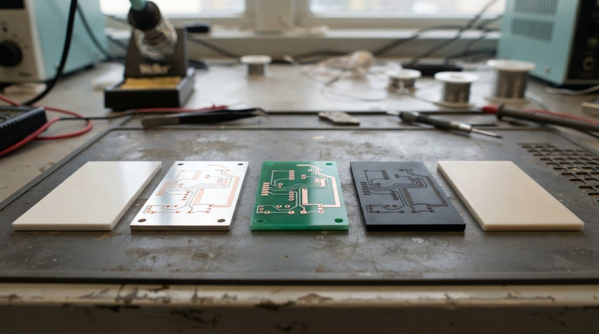
| Parameter | 96% Al2O3 | 99.6% Al2O3 | AlN | Metal-core (Al) | FR-4 |
|---|---|---|---|---|---|
| Thermal conductivity (W/m·K, 25 °C) | 24–28 | 28–33 | 170–200 | 1–2 (dielectric layer) | 0.25–0.3 |
| CTE (ppm/°C) | 6.5–7.2 | 6.5–7.0 | 4.5–5.0 | 22–24 | 14–17 |
| Max. use temp. (substrate) | > 1 000 °C | > 1 000 °C | > 1 000 °C | ~150 °C | 130 °C (Tg) |
| Dielectric strength (kV/mm) | 14–16 | 15–17 | 14–17 | 3–6 | 20–40 |
| Relative cost per cm² | 1× | 1.3–1.5× | 3–5× | 0.3–0.5× | 0.05–0.1× |
Typical values for commercially available material, for comparison only. Confirm against the datasheet for your specific grade.
For designs where the substrate Rth is not the bottleneck—say, a sensor interface dissipating under 2 W—96% alumina handles the thermal load easily and costs far less than AlN. If you need more detail on the higher-purity grade, see the page on 99.6% alumina thermal properties.
When NOT to Use 96% Alumina
Heat flux above ~80 W/cm². At this density, the substrate temperature rise through even a 0.38 mm alumina layer becomes significant. AlN or Si3N4 with DBC/AMB metallisation is the standard choice for IGBT modules and SiC half-bridges in this range.
CTE-critical bare-die attach for large silicon or SiC devices. Silicon’s CTE is ~3 ppm/°C. Alumina at 6.5–7.2 ppm/°C creates enough mismatch to crack large die (>10 mm edge) under thermal cycling. AlN (4.5–5.0 ppm/°C) is a closer match.
Cost-sensitive, low-power consumer electronics. If your board runs below 130 °C and FR-4 or a metal-core PCB meets thermal requirements, the 10–50× cost premium of ceramic is hard to justify.
High-frequency RF above ~20 GHz. Alumina’s dielectric constant (~9.6) and loss tangent (~0.0002–0.001 at 1 MHz) are acceptable for many RF designs, but above 20 GHz, lower-Dk substrates (quartz, Rogers RO4000 series) may give better insertion-loss performance.
FAQ
Does 96% alumina crack from thermal shock?
96% alumina withstands thermal shock of approximately 200–250 °C ΔT (per CeramTec Rubalit 708S data). Standard reflow soldering profiles (peak ~260 °C, ramp ≤ 3 °C/s) are well within this limit. Rapid quench from above 400 °C can cause fracture, so avoid direct flame or uncontrolled cooling in process.
Can I use 96% alumina for a DBC substrate?
Yes. Direct bond copper (DBC) on 96% alumina is a mature, widely available process. Copper is bonded at roughly 1 065 °C using a Cu-O eutectic. The resulting bond strength exceeds 8 N/mm (peel) and handles thermal cycling from −55 to +150 °C for thousands of cycles per IEC 60749-34.
How does 96% alumina compare to 99.6% alumina thermally?
99.6% alumina offers 28–33 W/m·K versus 24–28 W/m·K for 96%—roughly a 15–20 % improvement. The higher-purity grade also has slightly lower dielectric loss. For most designs, the thermal gain does not justify the 30–50 % cost increase unless you also need the tighter dimensional tolerances that come with the higher-purity material.
What solder alloys work on alumina ceramic PCBs?
Standard SAC305 (Sn-Ag-Cu) reflow works on metallised alumina. For higher operating temperatures, Au-Sn (80/20, melting at 280 °C) or Au-Ge (88/12, melting at 361 °C) alloys are common. The limiting factor is the metallisation adhesion and barrier layers, not the ceramic itself.
Is 96% alumina suitable for automotive under-hood electronics?
Yes. Alumina substrates routinely qualify to AEC-Q200 and operate continuously at 150–200 °C ambient in engine-bay sensor modules, ignition drivers, and exhaust-gas sensor interfaces. The ceramic and DBC metallisation handle the thermal cycling (−40 to +150 °C, 1 000+ cycles) required by AEC-Q100 Grade 0.
Next Step
If your alumina 96% Al2O3 thermal design model shows the material fits your power budget, the next step is to pin down substrate thickness, copper weight, and surface finish. For a broader view of how ceramic substrates manage heat across different materials, see the thermal management with ceramic PCBs overview. When you are ready to get pricing on a specific design, request a quote with your Gerber files and thermal requirements.