A solderability test measures how readily molten solder wets a metallised surface on a ceramic substrate. Ceramic base materials (Al₂O₃, AlN, Si₃N₄) are inherently non-wettable, so solderability depends entirely on the metallisation and surface finish. If either is degraded by oxidation, contamination, or poor adhesion, solder joints fail during assembly or in the field. Testing before assembly catches these problems when rework is still cheap.
Key Takeaways
- The three standard solderability test methods are dip-and-look, wetting balance (meniscograph), and surface mount simulation per J-STD-002 and IPC-TM-650 2.4.14.
- Acceptance typically requires ≥ 95 % wetting coverage on the test area, with no dewetting or non-wetting exceeding 5 % of the pad.
- Steam ageing (8 hours, 93 °C ± 2 °C per J-STD-002) simulates shelf-life degradation and is the most common pre-conditioning step.
- Ceramic substrates with ENIG or ENEPIG finishes generally pass solderability after 12+ months of storage; bare nickel or bare copper finishes degrade faster and need tighter incoming inspection.
Why Ceramic Substrates Need a Solderability Test
On an FR-4 board, copper pads are electroplated directly onto the laminate. On a ceramic PCB, metallisation is applied by thick-film screen printing, thin-film sputtering, or copper plating processes onto a fired ceramic body. Each method introduces its own adhesion and surface-condition variables. A pad that looks fine under magnification can still refuse to wet if the metallisation is under-fired, if flux residues from a previous step remain, or if a thin oxide layer has formed during storage.
Solderability testing is especially important for high-reliability assemblies in power electronics, aerospace, and medical devices, where rework on a ceramic board is difficult or impossible. It is also critical after long storage periods or when changing surface finish suppliers.
Standard Test Methods
Dip-and-Look (IPC-TM-650, Method 2.4.14)
The test coupon or a representative pad area is fluxed, dipped into a solder pot (typically Sn63/Pb37 at 245 °C ± 5 °C for leaded, or SAC305 at 255 °C ± 5 °C for lead-free) for a specified dwell time (usually 5 ± 0.5 seconds), then withdrawn and inspected visually. Acceptance per IPC/EIA J-STD-002 Class 3 requires ≥ 95 % of the test surface to be covered with a smooth, continuous solder film, with no pinholes, dewetting, or non-wetting exceeding 5 % of the area.
This is the simplest and most common method. Its weakness is subjectivity: two inspectors can disagree on borderline results. For that reason, many specs require photographic documentation of every test coupon.
Wetting Balance (Meniscograph) Analysis
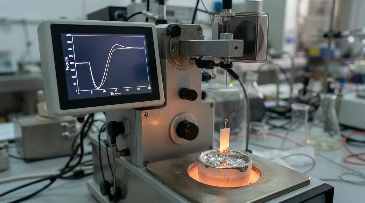
A wetting balance test is quantitative. The coupon is suspended from a sensitive force transducer and lowered into the solder bath at a controlled speed. The instrument records force versus time, producing a wetting curve. Key parameters extracted from the curve include:
- t₀ — time to zero force (buoyancy equals wetting force), typically required to be < 1.0 s for a well-finished ceramic pad.
- F_max — maximum wetting force, proportional to the contact angle and surface tension.
- Wetting time (t₂) — time to reach two-thirds of F_max, a measure of wetting speed.
Wetting balance data removes inspector subjectivity and provides lot-to-lot trending. It is the preferred method for qualifying a new ceramic substrate material or surface finish combination.
Surface Mount Simulation (Reflow Solderability)
For substrates destined for SMT assembly, a solder paste print and reflow profile can be used as a solderability test. Solder paste is stencil-printed onto test pads, reflowed per the paste manufacturer’s profile, and inspected for wetting, voiding, and solder ball formation. This method tests the real-world interaction between the paste, flux chemistry, and the substrate finish under actual thermal conditions.
Pre-Conditioning: Simulating Shelf Life
Raw solderability on a freshly finished board is rarely the concern. The real question is whether the finish will still wet after weeks or months in storage. J-STD-002 defines several ageing categories:
| Category | Condition | Duration | Simulated Shelf Life |
|---|---|---|---|
| 1 | As received (no ageing) | — | Immediate |
| 2 | Steam ageing, 93 °C ± 2 °C, 95 % RH | 8 h | ~6-12 months typical storage |
| 3 | Steam ageing, 93 °C ± 2 °C, 95 % RH | 16 h | Extended storage / harsh environment |
Conditions per J-STD-002E. Simulated shelf life is approximate and depends on packaging and environment.
For ceramic substrates with bare thick-film metallisation (e.g., tungsten or molybdenum-manganese), even Category 2 ageing can push results below the acceptance threshold. Adding a nickel barrier and gold or tin flash dramatically improves post-ageing solderability. ENIG finishes (3-5 µm Ni, 0.05-0.1 µm Au) routinely pass Category 3 ageing with > 98 % wetting coverage.
Common Failure Modes on Ceramic PCBs
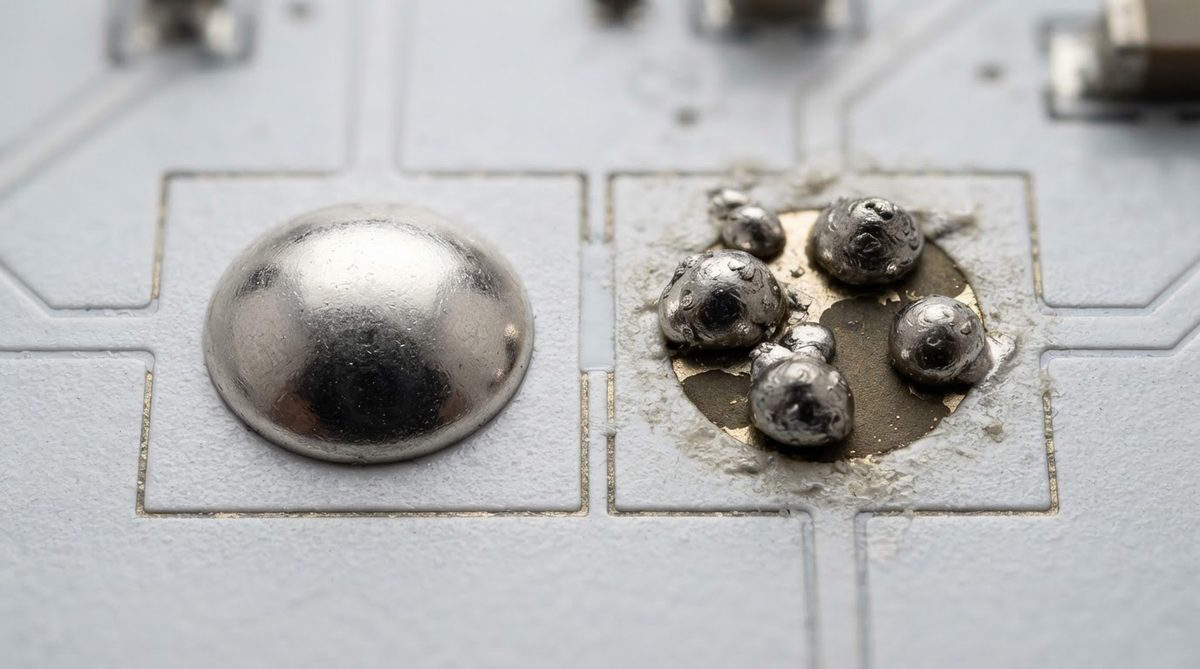
Non-wetting. Solder does not spread onto the pad at all. Root causes: oxidised or contaminated metallisation, under-fired thick-film paste, or a surface finish that has been consumed (e.g., immersion tin fully converted to intermetallic).
Dewetting. Solder initially wets, then pulls back, leaving irregular mounds with exposed base metal. This often indicates a thin contaminant layer or poor metallisation adhesion. Dewetting is harder to detect visually than non-wetting and is a leading cause of field solder joint failures.
Solder balling / bridging. Seen mainly in the reflow simulation method. Usually caused by excessive oxide on the finish or incompatible flux chemistry rather than a true metallisation defect.
When failures occur, cross-sectioning the pad and examining the metallisation stack under SEM/EDS is the fastest way to identify the root cause. Traceability back to the substrate lot is essential for containment. A robust lot traceability system lets you isolate affected boards quickly.
Worked Example: Incoming Inspection Sampling
Suppose you receive a lot of 500 alumina substrates with ENIG finish for a Class 3 medical assembly. Per IPC J-STD-002 and your internal spec, you require Category 2 steam ageing followed by dip-and-look with ≥ 95 % wetting. Using ANSI/ASQ Z1.4 Level II, normal inspection, AQL 1.0 %, the sample size code for a lot of 500 is H (sample size 50). Accept on 1 defective, reject on 2. You steam-age 50 coupons for 8 hours at 93 °C, dip-test, and photograph each result. If 0 or 1 coupons show < 95 % wetting, the lot passes. If 2 or more fail, you reject the lot and request a corrective action from the substrate supplier.
When Solderability Testing Is Not Necessary
If your ceramic substrate will be joined by epoxy die attach, wire bonding only, or sintered silver, a solder wetting test adds cost without value. Likewise, bare ceramic substrates used as heat spreaders with no metallisation do not require solderability screening. For low-volume prototypes assembled within days of receiving boards, the risk of storage degradation is minimal, and a visual check of pad appearance may suffice. Save formal solderability testing for production lots, long-stored inventory, and Class 2/3 reliability requirements.
Relationship to Other Reliability Tests
Solderability testing validates the initial joint. It does not guarantee long-term reliability under thermal stress. For that, you need thermal cycling reliability testing and, where rapid temperature excursions are expected, thermal shock test methods. A substrate that passes solderability but has poor metallisation adhesion may survive assembly yet fail after 500 thermal cycles. Use solderability as one gate in a broader qualification sequence, not the only one.
FAQ
Can you perform a solderability test on a finished ceramic PCB instead of a coupon?
Yes, but it is destructive. The dip-and-look test coats the pad with solder, making it unusable for its intended component. Most engineers test dedicated coupons processed alongside the production panel, so the boards themselves remain unaffected.
Does lead-free solder change the acceptance criteria?
The wetting coverage threshold (≥ 95 %) stays the same under J-STD-002, but the solder bath temperature increases from 245 °C to 255 °C for SAC305. Higher temperature and lower wetting force of lead-free alloys make marginal finishes more likely to fail. Expect slightly longer wetting times on the meniscograph curve.
How often should I retest stored ceramic substrates?
Industry practice is to retest solderability if boards have been stored longer than the qualified shelf life of the surface finish. For ENIG, that is typically 12 months in sealed moisture-barrier bags. For OSP or immersion tin, retest after 3-6 months. Always retest after any breach of the sealed packaging.
What flux type should be used during the test?
J-STD-002 specifies a non-activated (R or ROL0) flux for the standard test so that the flux does not mask a marginal finish. Using a more aggressive flux (e.g., RA or ORL1) during the test may produce passing results that do not reflect real assembly conditions, especially if your production process uses a mild no-clean flux.
Is wetting balance testing worth the equipment cost for a small operation?
A meniscograph system costs roughly $15,000-$40,000. If you test fewer than a few hundred lots per year, outsourcing to a third-party lab is more practical. Labs accredited to IPC-TM-650 or J-STD-002 can return results in 3-5 business days.