Copper peel strength on ceramic substrates typically ranges from 0.8 kN/m for thin-film or DPC metallization up to 2.0 kN/m or higher for AMB (active metal brazing), measured per IPC-TM-650 2.4.8 at 90° peel angle and 50 mm/min crosshead speed. The copper peel strength ceramic engineers need depends on the metallization process, the ceramic grade, copper thickness, and the thermal cycling profile the board will see in service.
Key Takeaways
- AMB on Si₃N₄ delivers the highest copper peel strength among ceramic metallization methods, commonly 1.5–2.0+ kN/m per IPC-TM-650 2.4.8.
- DBC (direct bond copper) on Al₂O₃ 96% typically yields 1.0–1.5 kN/m; on AlN, 0.8–1.3 kN/m.
- DPC (direct plated copper) and sputtered thin-film metallizations start lower, often 0.6–1.0 kN/m, but are adequate for most signal-level and fine-line applications.
- Peel strength after thermal cycling matters more than the as-received value. A 10–20% drop after 1,000 cycles (–40 °C to +150 °C) is typical for DBC on alumina.
- The most common failure mode in a well-bonded DBC joint is cohesive fracture within the ceramic, not adhesive failure at the copper–oxide interface.
What Copper Peel Strength on Ceramic Measures
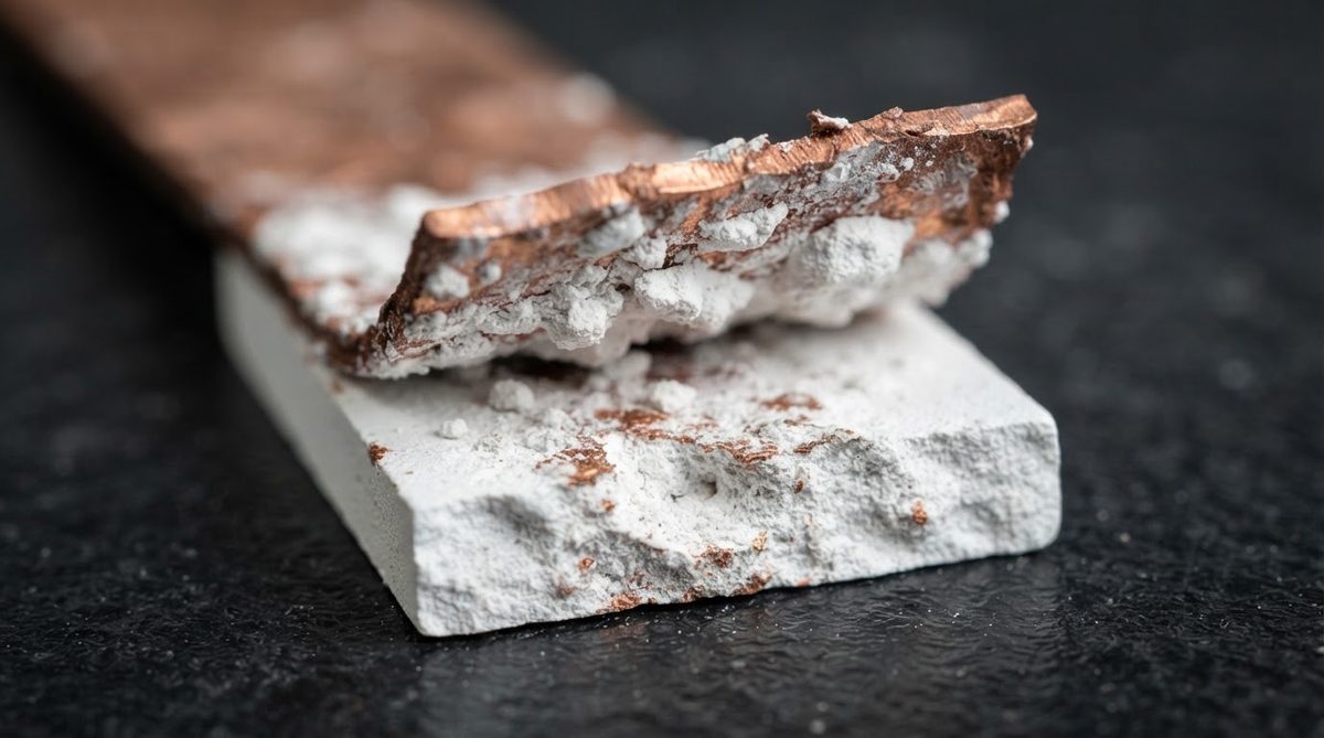
Peel strength quantifies the force per unit width needed to pull a copper foil or metallization layer away from a substrate at a defined angle, usually 90°. It is reported in kN/m (or the older unit lbf/in; 1 kN/m ≈ 5.71 lbf/in). The test captures the combined effect of chemical bonding, mechanical interlocking, and any interfacial reaction layer between copper and ceramic.
Peel strength is not the same as shear strength or tensile pull strength, both of which are sometimes specified for die-attach or wire-bond pads. For large-area copper planes on power substrates, peel is the standard metric because it mimics the stress state created by CTE mismatch during thermal cycling: the copper tries to lift at the edges of the bonded area.
Standard Test Methods for Copper Peel Strength on Ceramic Substrates
Two test standards dominate the industry:
| Standard | Peel Angle | Crosshead Speed | Specimen Width | Notes |
|---|---|---|---|---|
| IPC-TM-650 2.4.8 | 90° | 50 mm/min | 3.18 mm (0.125 in) typical | Most widely cited for PCBs; references IPC-6012 acceptance criteria |
| DIN EN 2243-2 | 90° or 180° | 100 mm/min | 25 mm | Common in European automotive and industrial specs |
Typical test parameters for reference only. Always specify the exact standard revision, angle, speed, and specimen geometry in your purchase spec.
Specimen preparation matters as much as the test itself. The copper strip must be defined by etching or laser cutting, not by mechanical scoring, which can pre-crack the ceramic and depress the measured value. The substrate should be fixtured flat, with no bending moment applied outside the peel zone. Results from a curved or unsupported substrate are not comparable to flat-fixture data.
Typical Copper Peel Strength Values by Ceramic Metallization Process
| Process | Substrate | Cu Thickness | Peel Strength (kN/m) | Condition | Source |
|---|---|---|---|---|---|
| DBC | Al₂O₃ 96% | 300 µm | 1.0–1.5 | As-received, 90° peel, 50 mm/min | Rogers curamik datasheet |
| DBC | AlN | 300 µm | 0.8–1.3 | As-received, 90° peel, 50 mm/min | Rogers curamik datasheet |
| AMB | Si₃N₄ | 300 µm | 1.5–2.0+ | As-received, 90° peel, 50 mm/min | Kyocera SN series datasheet |
| AMB | AlN | 300 µm | 1.2–1.8 | As-received, 90° peel, 50 mm/min | Kyocera datasheet |
| DPC (sputtered + plated) | Al₂O₃ 96% | 50–100 µm | 0.6–1.0 | As-received, 90° peel, 50 mm/min | Industry consensus; varies by seed layer |
| Thick film (Ag/Pd fired) | Al₂O₃ 96% | 10–15 µm | 0.3–0.8 | As-received, 90° peel | DuPont / Heraeus paste datasheets |
Typical values for commercially available material, for comparison only. Confirm against the datasheet for your specific grade.
The large spread within each row reflects real variation in surface roughness, firing profile, oxide layer thickness (for DBC), and braze alloy composition (for AMB). Specifying a minimum copper peel strength in your ceramic substrate drawing is more useful than targeting a single number. For power modules per automotive AQG 324, a post-cycling minimum of 0.8 kN/m is a common gate.
Why Copper Peel Strength Varies on Ceramic Substrates
Ceramic Surface Condition
A rougher ceramic surface (Ra 0.4–0.8 µm) gives more mechanical interlocking and generally higher peel values than a polished surface (Ra < 0.1 µm). However, excessive roughness can introduce micro-cracks that become failure initiation sites under thermal cycling. The optimum is process-dependent. DBC bonds benefit from a controlled surface roughness in the 0.3–0.6 µm Ra range, per published data from CoorsTek and Maruwa.
Copper Thickness
Thicker copper (300 µm vs. 127 µm) stores more elastic energy during peel, which can slightly increase the measured peel force but also increases the CTE-mismatch stress in service. For copper plating processes and tolerances, the seed-layer adhesion is the weak link, not the bulk plated copper.
Thermal History
Post-solder reflow and thermal cycling reliability testing degrade peel strength. A well-made DBC on Al₂O₃ 96% will retain 80–90% of its initial peel strength after 1,000 cycles from –40 °C to +150 °C (per JEDEC JESD22-A104). AMB on Si₃N₄ retains a higher fraction because Si₃N₄’s fracture toughness (6–7 MPa·√m vs. 3.5–4 MPa·√m for alumina) resists crack growth at the interface.
Worked Example: Specifying Copper Peel Strength for a Ceramic Power Module
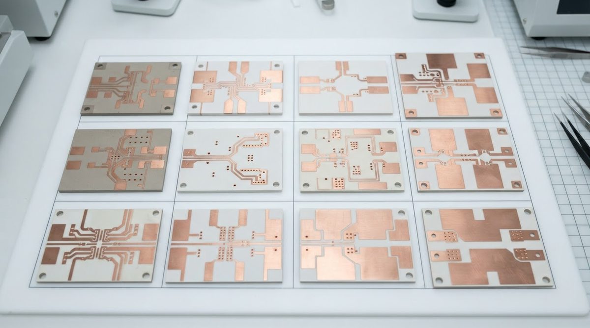
Suppose you are designing a SiC half-bridge module for a traction inverter. The substrate is DBC on Al₂O₃ 96%, 300 µm Cu on both sides. The qualification spec requires thermal cycling per AQG 324: 1,000 cycles, –40 °C to +150 °C, 3 min dwell.
- As-received minimum peel: Specify ≥ 1.2 kN/m at 90° per IPC-TM-650 2.4.8. This sits comfortably within the 1.0–1.5 kN/m range for DBC on alumina and allows for normal lot-to-lot variation.
- Post-cycling minimum peel: Specify ≥ 0.9 kN/m after 1,000 cycles. This implies no more than 25% degradation from the as-received floor.
- Failure mode requirement: Require that at least 80% of the fracture surface shows cohesive ceramic failure (white residue on the copper strip), not clean adhesive separation (shiny copper with no ceramic residue). Cohesive failure means the bond is stronger than the ceramic itself.
- Sample size: 5 strips per lot, from the panel edge and center, to catch any gradient in bonding temperature across the furnace.
If your application sees higher junction temperatures or deeper thermal swings (e.g., –55 °C to +175 °C for aerospace), consider AMB on Si₃N₄ and raise the post-cycling floor to ≥ 1.2 kN/m. The thermal shock and cycling test methods page covers how to define those profiles.
Common Failure Modes in Peel Testing
Cohesive ceramic fracture. The crack runs through the ceramic a few micrometres below the interface. This is the desired failure mode for DBC and AMB. It means the metal–ceramic bond exceeded the ceramic’s own strength.
Adhesive failure at the interface. The copper peels cleanly with no ceramic residue. This indicates a weak bond, often caused by contamination, insufficient oxide layer (DBC), or incomplete braze wetting (AMB). Reject the lot.
Copper foil tearing. The copper tears before the bond fails. This happens with very thin copper (< 100 µm) or when the strip width is too narrow. It means the test did not actually measure the bond, so the result is invalid. Widen the strip or use a thicker foil for the test coupon.
When Peel Strength Is Not Your Main Concern
Copper peel strength on ceramic is critical for power substrates with large copper areas subject to CTE-driven stress. It is less relevant in these cases:
- Thin-film RF circuits on alumina or AlN. Metallization is typically < 10 µm. Adhesion is verified by tape test (ASTM D3359) or scratch test, not 90° peel, because the copper is too thin to peel without tearing.
- LTCC multilayer boards. Conductor adhesion is tested by wire-bond pull or solder joint shear, not peel, because the conductors are co-fired screen-printed traces, not foil.
- FR-4 or metal-core PCBs. If your operating temperature stays below 130 °C and thermal cycling is mild, standard FR-4 copper adhesion (≥ 0.7 kN/m per IPC-6012 Class 2) is adequate and far cheaper. Ceramic substrates are justified when the thermal, frequency, or hermeticity requirements rule out organic laminates.
Frequently Asked Questions
Does copper peel strength on ceramic change after soldering?
Yes. A standard SAC305 reflow profile (peak 245 °C, ~60 s above liquidus) typically reduces peel strength by 5–10% on DBC substrates. The reduction comes from additional thermal stress and minor oxidation at the bond interface. Always measure peel strength on post-reflow coupons if your spec requires it.
Can I compare peel strength values tested at 90° and 180°?
Not directly. A 180° peel test on the same specimen will usually give a lower force reading than a 90° test because the geometry changes how energy is distributed between bending and interfacial fracture. Always compare values taken at the same angle and crosshead speed.
What peel strength do I need for wire bonding?
Wire-bond reliability depends more on the surface finish and pad metallurgy than on bulk peel strength. A DPC pad with 0.6 kN/m peel strength can support reliable Au or Al wire bonds if the surface finish (e.g., ENIG or ENEPIG) is within spec. Use wire-bond pull and shear tests per MIL-STD-883 Method 2011 to qualify the pad, not peel testing. For guidance on verifying solder and bond pad quality, see ceramic substrate solderability tests.
How do I inspect bond quality without destroying the board?
Scanning acoustic microscopy (SAM) can detect delaminations and voids at the copper–ceramic interface non-destructively. X-ray inspection for vias and bond layers is useful for checking braze coverage on AMB substrates but does not directly measure adhesion. Peel testing remains destructive and is performed on sacrificial coupons from the same production lot.
Is higher copper peel strength always better on ceramic?
Not necessarily. Extremely high bond strength (> 2.5 kN/m) can mean the ceramic fractures catastrophically during thermal events rather than allowing controlled micro-cracking that relieves stress. For Si₃N₄ AMB substrates, the high fracture toughness of the ceramic makes this less of a concern, but for Al₂O₃ DBC, an excessively thick Cu₂O bonding layer that raises initial peel can also make the substrate more brittle under cycling.
Next Step
If you are specifying a ceramic substrate and need copper peel strength data for a specific metallization and ceramic combination, request a test coupon with your production lot. For thermal conductivity data across ceramic grades, see our reference table. Ready to get numbers for your project? Submit your files for a quote and we will include peel-strength certification in the deliverables.