Silicon nitride Si3N4 AMB active metal brazing substrates pair the toughest structural ceramic available for electronics with copper layers bonded through an Ag-Cu-Ti braze alloy, producing power-module carriers that survive 3,000+ thermal cycles from −40 °C to +250 °C where alumina or aluminum nitride DBC substrates would crack. The combination is expensive, but for EV traction inverters, rail converters, and aerospace power stages, nothing else delivers the same reliability margin.
What Is a Silicon Nitride Si3N4 AMB Active Metal Brazing Substrate?
A silicon nitride Si3N4 AMB active metal brazing substrate is a ceramic circuit carrier made from a silicon nitride base plate with copper foil bonded to one or both faces using an active metal braze alloy, typically Ag-Cu-Ti. The titanium in the braze reacts with the ceramic surface at 800–900 °C in vacuum, forming a TiN reaction layer that creates a true metallurgical bond between the copper and the Si3N4.
Unlike Si3N4 DBC (direct bonded copper), which relies on a Cu-O eutectic at ~1,065 °C, the AMB process operates at a lower brazing temperature and produces a more ductile interface. That ductile braze layer absorbs CTE mismatch stress between copper (17 ppm/K) and Si3N4 (2.7 ppm/K), which is why silicon nitride Si3N4 AMB active metal brazing substrates tolerate thicker copper—up to 800 µm or even 1,200 µm per side—without delamination.
Why Choose Silicon Nitride for AMB Over AlN or Al2O3?
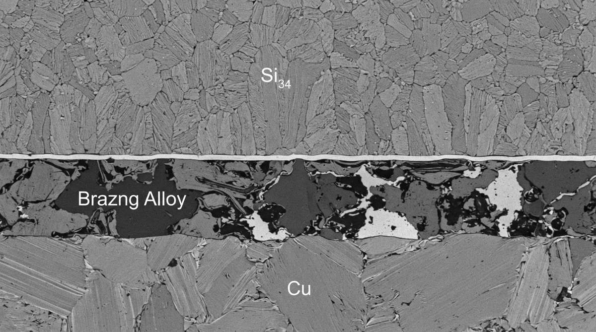
The answer is mechanical toughness. Si3N4 has a fracture toughness of 6–7 MPa·√m versus 2.5–3.5 MPa·√m for AlN and 3.5–4.0 MPa·√m for 96% Al2O3 (per CoorsTek and Kyocera published datasheets). In power modules that see thousands of on/off cycles, this toughness translates directly into longer substrate life before crack initiation.
The trade-off is Si3N4 thermal conductivity: 70–90 W/m·K for high-purity grades, compared with 170–200 W/m·K for AlN. You compensate by using thinner Si3N4 substrates (0.25–0.32 mm) and thicker copper, which spreads heat laterally before it enters the ceramic. The net thermal resistance can approach that of a thicker AlN DBC stack, while the mechanical reliability far exceeds it.
| Parameter | Si3N4 AMB | AlN AMB | Al2O3 DBC | Unit | Condition / Source |
|---|---|---|---|---|---|
| Thermal conductivity | 70–90 | 170–200 | 24–28 | W/m·K | 20 °C; Kyocera SN series / CoorsTek datasheets |
| Flexural strength | 600–900 | 300–400 | 300–380 | MPa | 3-pt bend, ASTM C1161 |
| Fracture toughness | 6–7 | 2.5–3.5 | 3.5–4.0 | MPa·√m | ASTM C1421 |
| CTE | 2.7 | 4.5 | 7.2 | ppm/K | 25–400 °C |
| Max copper thickness (AMB) | 800–1,200 | 600–800 | N/A (DBC: 300) | µm | Manufacturer typical |
| Thermal cycle life (−40/+250 °C) | >3,000 | 500–1,500 | 200–500 | cycles to 10% delam. | Industry test data, Heraeus / Rogers reports |
Typical values for commercially available material, for comparison only. Confirm against the datasheet for your specific grade.
How the Silicon Nitride Si3N4 AMB Active Metal Brazing Process Works
Active metal brazing follows a well-defined sequence. The ceramic substrate is first lapped to a controlled flatness, typically < 25 µm TTV. A thin foil of Ag-Cu-Ti braze alloy (often 70Ag-27Cu-3Ti, roughly 50 µm thick) is placed between the ceramic and the copper foil. The entire stack enters a vacuum furnace at 10⁻⁴–10⁻⁵ mbar.
The furnace ramps to 800–900 °C and holds for 10–30 minutes. Titanium migrates to the ceramic surface, reacts to form TiN, and the Ag-Cu matrix wets the resulting layer. After controlled cooling, the copper is patterned by photolithography and etching, then circuits are plated or finished. For a broader look at how ceramic boards move from design files to finished parts, see the PCB manufacturing process overview.
Worked Example: Thermal Resistance Through an Si3N4 AMB Stack
Consider a 10 mm × 10 mm die on a 0.32 mm Si3N4 substrate with 0.3 mm copper on each side. Assume Si3N4 k = 85 W/m·K and Cu k = 390 W/m·K.
One-dimensional thermal resistance of each layer through a 10 × 10 mm footprint (area = 1 × 10⁻⁴ m²):
- Top Cu: R = 0.0003 / (390 × 1 × 10⁻⁴) = 0.0077 K/W
- Si3N4: R = 0.00032 / (85 × 1 × 10⁻⁴) = 0.0376 K/W
- Bottom Cu: R = 0.0003 / (390 × 1 × 10⁻⁴) = 0.0077 K/W
- Total stack: ~0.053 K/W
At 200 W dissipation, the temperature drop across the substrate stack alone is roughly 10.6 °C. A comparable 0.63 mm AlN DBC (k = 180, Cu 0.3 mm) gives ~0.050 K/W—nearly identical—but the AlN version will crack far sooner under deep thermal cycling. This is the core engineering case for silicon nitride Si3N4 AMB active metal brazing in high-reliability power modules.
Enter your substrate dimensions, copper thickness, and dissipated power below to estimate the temperature rise across your own Si3N4 AMB stack.
When NOT to Use Si3N4 AMB
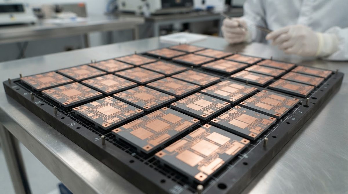
Silicon nitride Si3N4 AMB active metal brazing substrates cost 3–8× more than Al2O3 DBC per unit area, depending on copper thickness and volume. If your module operates within a mild thermal cycle range (−20 °C to +125 °C) and does not require more than 300 µm copper, alumina DBC or even aluminum MCPCB may be sufficient and far cheaper.
For applications where raw thermal conductivity matters more than mechanical cycling—steady-state high-power LEDs or RF loads without frequent on/off transients—AlN AMB substrates will outperform on thermal resistance at lower cost than Si3N4. Choose Si3N4 specifically when cycle life and crack resistance dominate your failure-mode analysis.
If your design needs only thin metallization and fine traces (< 100 µm line/space), DPC (direct plated copper) on alumina or AlN is a better fit. AMB is optimized for thick copper power circuits, not high-density signal routing.
Selecting Substrate Thickness and Size
Most Si3N4 AMB substrates ship on 0.25 mm or 0.32 mm ceramic. Thinner substrates lower thermal resistance but are more fragile during handling before copper bonding. After bonding, the copper stiffens the assembly substantially. Check the ceramic substrate thickness options to match your mechanical and thermal requirements.
Panel sizes for AMB are constrained by furnace dimensions and braze uniformity. Common working sizes range from 50 × 50 mm to 190 × 140 mm per substrate unit, with larger panels available for high-volume production.
Frequently Asked Questions
Can Si3N4 AMB substrates be used above 300 °C continuously?
The Si3N4 ceramic itself is stable well above 1,000 °C, but the Ag-Cu-Ti braze joint limits continuous use to roughly 300–350 °C. Beyond that temperature the braze alloy softens and copper oxidation accelerates, degrading the bond. For higher temperatures, look at refractory metal metallization on bare ceramic.
Is Si3N4 AMB available with copper on only one side?
Yes. Single-sided AMB is used for heatsink-attach applications where the backside bonds directly to a baseplate. However, double-sided copper is more common because the symmetric structure balances residual stress and reduces substrate warpage after brazing.
How do you solder components to an Si3N4 AMB substrate?
Standard Sn-Ag-Cu (SAC) solder or high-temperature Pb-based solder (for automotive-grade modules) works on AMB copper surfaces finished with Ni/Au or Ni/Ag plating. Die attach via sintered silver paste is increasingly common for SiC and GaN devices on Si3N4 AMB because it eliminates solder fatigue as a failure mode.
What is the typical lead time for Si3N4 AMB prototypes?
Prototype quantities (5–25 pieces) typically ship in 4–6 weeks from approved artwork, depending on copper thickness and surface finish. Production volumes with established tooling can run 6–10 weeks. Lead times are longer than Al2O3 DBC because fewer facilities worldwide run Si3N4 AMB in volume.
Does Si3N4 AMB replace wire bonding?
No. AMB defines how copper is attached to the ceramic. Wire bonding or ribbon bonding is still used to connect die pads to the copper traces on the AMB substrate. Some designs replace wire bonds with copper clip soldering, but that is a separate packaging choice, not an AMB feature.