In a PCB on heatsink assembly, the substrate is the last solid barrier between a hot die and the cooling surface. A 1.0 mm FR-4 layer contributes roughly 33 °C/W per cm² of contact area (thermal conductivity ~0.3 W/mK), while a 0.635 mm alumina 96% ceramic substrate contributes about 0.24 °C/W per cm² (24–28 W/mK). Choosing the right substrate material and attach method determines whether mounting a PCB on heatsink actually delivers the thermal performance you expect.
Why the Substrate Dominates PCB on Heatsink Thermal Resistance
A typical PCB on heatsink thermal stack has four layers between the die junction and the heatsink surface: die attach (solder or epoxy), the substrate itself, a thermal interface material (TIM), and the heatsink contact surface. In most designs, the substrate and the TIM together account for 60–80% of the total junction-to-sink thermal resistance (Rθ,j-s). The heatsink-to-ambient portion is a separate problem solved by fin geometry and airflow. The substrate portion is a materials problem.
For power semiconductors dissipating 10 W or more per cm², even small differences in substrate thermal conductivity translate to large differences in junction temperature. A 10 °C reduction in Tj can double the projected lifetime of a SiC MOSFET, per Arrhenius-based reliability models referenced in JEDEC JEP122H.
Thermal Resistance Comparison: FR-4, MCPCB, and Ceramic Substrates
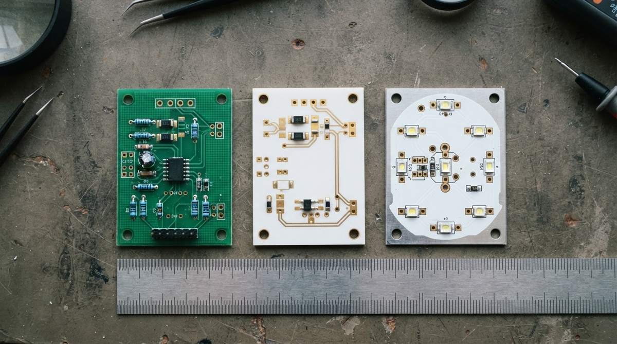
The one-dimensional conduction resistance through a flat substrate is Rθ = t / (k × A), where t is thickness, k is thermal conductivity, and A is the heat-spreading area. The table below compares common PCB on heatsink substrate options for a 10 mm × 10 mm footprint (1 cm²).
| Substrate | Thickness (mm) | k (W/mK) | Rθ (°C/W) | Condition | Source |
|---|---|---|---|---|---|
| FR-4 | 1.0 | 0.25–0.35 | 2.86–4.00 | 20 °C, per IPC-TM-650 2.4.8.2 | IPC-4101E typical values |
| Metal-core (Al base, dielectric 75 µm) | 0.075 dielectric | 1.0–3.0 | 0.25–0.75 | 20 °C | Bergquist/Henkel HT series datasheet |
| Al₂O₃ 96% | 0.635 | 24–28 | 0.23–0.26 | 20 °C, ASTM E1461 | CoorsTek ADS-96R datasheet |
| Al₂O₃ 99.6% | 0.635 | 28–35 | 0.18–0.23 | 20 °C, ASTM E1461 | Kyocera A-493 datasheet |
| AlN | 0.635 | 170–200 | 0.032–0.037 | 20 °C, ASTM E1461 | Maruwa AN-200 datasheet |
| Si₃N₄ | 0.32 | 85–90 | 0.036–0.038 | 20 °C, ASTM E1461 | Kyocera SN-90 datasheet |
Typical values for commercially available material, for comparison only. Confirm against the datasheet for your specific grade.
The key takeaway: a ceramic PCB on heatsink delivers substrate-layer thermal resistance 10–100× lower than FR-4, and 3–8× lower than a typical metal-core PCB dielectric layer. AlN and Si₃N₄ substrates approach negligible contribution to the total stack.
Enter your substrate area, thickness, and dissipated power below to estimate the junction-to-heatsink temperature rise for your own design.
Worked Example: 50 W IGBT on Three Substrate Types
Consider a 50 W IGBT die (10 mm × 10 mm) soldered to a substrate that is bolted to an aluminum heatsink through a 50 µm layer of thermal grease (k ≈ 5 W/mK). We want to find the temperature rise from the bottom of the die attach to the top of the heatsink (ΔTsubstrate+TIM).
TIM resistance (same for all): RTIM = 0.00005 m / (5 W/mK × 0.0001 m²) = 0.10 °C/W
FR-4 (1.0 mm): Rsub = 0.001 / (0.3 × 0.0001) = 33.3 °C/W → ΔT = 50 × (33.3 + 0.10) = 1,670 °C. This is physically absurd, confirming that FR-4 cannot conduct 50 W through 1 cm² without melting.
Al₂O₃ 96% DBC (0.635 mm): Rsub = 0.000635 / (26 × 0.0001) = 0.244 °C/W → ΔT = 50 × (0.244 + 0.10) = 17.2 °C. Manageable. An alumina 96% DBC substrate is a common, cost-effective choice for this power range.
AlN DBC (0.635 mm): Rsub = 0.000635 / (180 × 0.0001) = 0.035 °C/W → ΔT = 50 × (0.035 + 0.10) = 6.8 °C. At this level, the TIM dominates. Switching to solder attach (k ≈ 50 W/mK, R ≈ 0.01 °C/W) would bring ΔT down to 2.3 °C. An AlN DBC substrate is the standard for high-density power modules above 100 W/cm².
Attach Methods: How the PCB Meets the Heatsink
The interface between the ceramic PCB and the heatsink matters as much as the substrate itself. Three methods dominate:
- Thermal grease + mechanical clamp. Simplest to assemble and rework. Typical bond-line thickness 25–75 µm, effective thermal conductivity 1–5 W/mK depending on compound. Adds 0.05–0.75 °C/W per cm². Grease can pump out under thermal cycling.
- Solder attach. The ceramic backside is metallized (typically Ni/Au or Ag), then soldered directly to a nickel- or tin-plated heatsink. Bond-line thickness 25–100 µm, effective k of 20–50 W/mK for SAC305 or similar. Adds 0.005–0.05 °C/W per cm². Permanent. Rework requires reflow.
- Sintered silver. Pressure-assisted Ag sintering at 200–280 °C. Bond-line k of 100–250 W/mK. Adds < 0.01 °C/W per cm². Used in SiC and GaN power modules where every degree counts. Requires controlled atmosphere and specialized equipment.
For designs using Si₃N₄ AMB substrates, the active metal braze layer on the backside already provides a solderable or sinterable surface, simplifying the PCB on heatsink attach step.
Choosing the Right Ceramic Material for Your Heatsink Assembly
Material choice depends on three factors: power density, thermal cycling severity, and cost budget.
- Al₂O₃ 96% (DBC or AMB): Best value for power densities below ~50 W/cm². CTE of 6.5–7.0 ppm/°C matches common lead-free solders reasonably well. Start here unless analysis shows you need more.
- AlN (DBC, AMB, or thick film): Necessary above ~80 W/cm² or when junction temperature targets are tight. CTE of 4.5–5.0 ppm/°C is a close match to silicon (2.6 ppm/°C) and SiC (4.0 ppm/°C), reducing die-attach stress. An AlN thick film substrate can be a lower-cost entry point when full DBC copper thickness is not needed.
- Si₃N₄ (DBC or AMB): Fracture toughness of 6–7 MPa·√m (vs. 3–4 for Al₂O₃ and 2.5–3.5 for AlN per ASTM C1421) makes it the choice for extreme thermal cycling (–55 °C to +175 °C, thousands of cycles). Common in EV traction inverters and railway power modules.
CTE Mismatch: The Hidden Failure Mode in PCB on Heatsink Assemblies
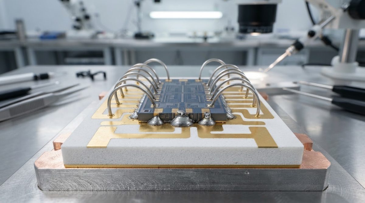
Bolting or soldering a ceramic PCB on heatsink creates a large CTE mismatch. Alumina sits at 6.5–7.0 ppm/°C; AlN at 4.5–5.0 ppm/°C. An aluminum heatsink is around 23 ppm/°C. Over repeated thermal cycles, this mismatch generates shear stress in the solder or TIM layer that can crack joints or delaminate the interface.
Mitigations include: using a compliant TIM (grease or phase-change material) instead of rigid solder; inserting a CTE-graded buffer layer such as a Cu-Mo-Cu composite (CTE ~7–9 ppm/°C); or switching to a copper heatsink (CTE ~17 ppm/°C), which reduces the mismatch by roughly 25% compared to aluminum. For solder-attached assemblies cycling more than 1,000 times over a ΔT > 100 °C, finite-element stress analysis of the interface is strongly recommended.
When Not to Use a Ceramic PCB on a Heatsink
Ceramic substrates add cost and design constraints. They are not always the right answer for a PCB on heatsink design.
- Power density below ~5 W/cm²: A standard metal-core PCB (MCPCB) with 1–3 W/mK dielectric handles LED arrays and low-power drivers at a fraction of the cost.
- Large board area with distributed low-power components: FR-4 with thermal vias under hot components, mounted on a heatsink with thermal grease, often suffices. Ceramic becomes expensive at board sizes above ~50 mm × 50 mm.
- Frequent mechanical shock or flex: Ceramic is brittle. If the assembly will see repeated bending, impact, or vibration beyond what the substrate’s flexural strength can handle (per ASTM C1161), a metal-core or flex-rigid PCB is safer.
- Rapid prototyping on a tight budget: Ceramic substrates have longer lead times and higher NRE than FR-4. If you are iterating the circuit weekly, prototype on FR-4 and switch to ceramic for qualification builds.
Frequently Asked Questions
Can I solder a ceramic PCB directly to an aluminum heatsink?
Yes, but the ceramic backside must be metallized first (typically with Ni/Au over a Ti/Cu or W/Ni seed layer), and the aluminum heatsink surface must be plated with nickel or tin to accept solder. Direct soldering to bare aluminum is not practical due to its native oxide layer.
Does thermal grease degrade over time between a ceramic PCB and a heatsink?
It can. Silicone-based greases tend to pump out under repeated thermal cycling, increasing thermal resistance by 20–50% over thousands of cycles. Phase-change materials and gap pads with mechanical retention resist pump-out better. For mission-critical applications, solder or sintered-silver attach eliminates this failure mode entirely.
What surface finish should the ceramic PCB have for heatsink mounting?
For solder attach, ENIG (electroless nickel/immersion gold) or electrolytic Ni/Au on the backside metallization is standard. For grease or pad interfaces, the finish matters less thermally, but a flat, lapped backside surface improves contact area. Surface roughness below Ra 0.8 µm is a common target for TIM interfaces.
How thin can a ceramic substrate be for a PCB on heatsink assembly?
Alumina substrates are commercially available down to 0.25 mm; AlN down to 0.32 mm; Si₃N₄ down to 0.20 mm. Thinner substrates reduce thermal resistance linearly but are more fragile during handling and assembly. For most heatsink-mounted power modules, 0.32–0.635 mm is the practical range, per datasheets from CoorsTek and Kyocera.
Is an AMB substrate better than DBC for heatsink mounting?
AMB (active metal brazing) allows thicker copper layers (up to 0.8 mm vs. ~0.3 mm for DBC) and stronger braze joints, which improves thermal spreading and cycling reliability. For high-current applications or assemblies that will see extreme thermal cycling, alumina AMB substrates or AlN AMB substrates offer measurable advantages over DBC. The trade-off is higher cost per unit.
Next Step
If you have a power dissipation target and a heatsink design, the next step is selecting the ceramic substrate material and metallization that fits your thermal budget. Review the SMD thermal jumper options for discrete thermal bridging, or request a quote with your board dimensions and power requirements at aluminapcb.com/instant-quote.