Copper metallized alumina is an alumina (Al₂O₃) ceramic substrate with copper conductors bonded directly to one or both faces. It delivers the full 401 W/mK thermal conductivity of bulk copper for heat spreading, while the alumina base provides dielectric isolation (≥ 8.5 kV/mm for 96% Al₂O₃) and a coefficient of thermal expansion (CTE) of 6.5–7.2 ppm/°C that sits closer to silicon and SiC than any metal-core board can.
Key Takeaways
- Four processes put copper onto alumina: DBC, DPC, AMB, and thick-film printing. Each targets a different copper thickness and feature resolution.
- DBC and AMB produce copper layers of 150–800 µm, suitable for high-current power modules carrying tens or hundreds of amps.
- DPC yields 1–200 µm copper with line/space down to 30–50 µm, ideal for fine-pitch LED arrays and RF circuits.
- Thick-film copper paste is the lowest-cost route but requires a nitrogen-atmosphere furnace to prevent oxidation, and conductivity is 60–80% of bulk copper.
- 96% alumina is the standard choice for copper metallized alumina substrates; 99.6% alumina adds roughly 15–20% better thermal conductivity (28–35 W/mK vs. 24–28 W/mK at 25 °C) at higher substrate cost.
What Is Copper Metallized Alumina?
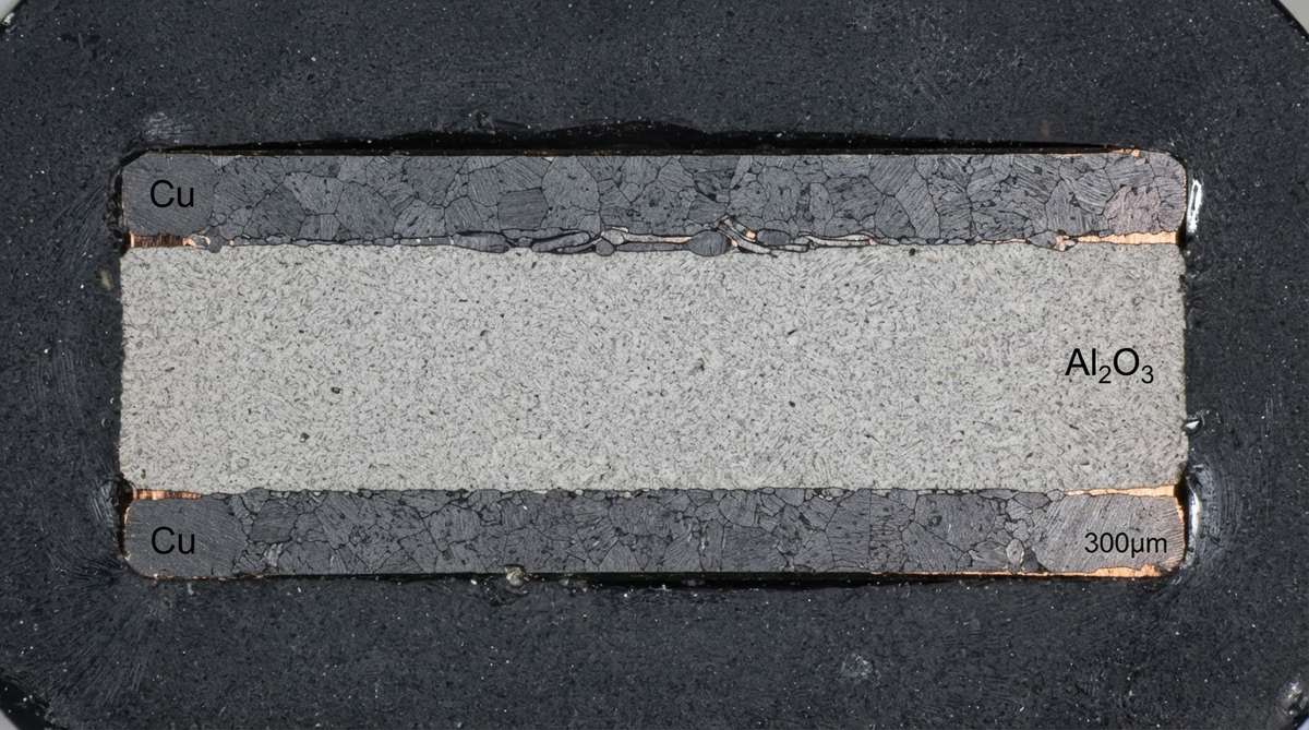
Copper metallized alumina is a ceramic substrate where copper conductor layers are formed on a fired alumina body through a bonding, plating, or printing process. Unlike organic PCBs, the ceramic carries no resin. The copper provides the circuit traces, ground planes, and thermal pads; the alumina provides mechanical support, electrical insulation, and a thermally stable platform.
The combination matters because copper alone warps under thermal cycling (CTE ~17 ppm/°C), while alumina alone cannot carry current. Bonding the two creates a substrate that handles high power density, survives wide temperature swings, and keeps leakage currents negligible even above 300 °C.
Four Methods for Producing Copper Metallized Alumina
The metallization method determines copper thickness, feature resolution, bond strength, and cost. Here is a direct comparison.
| Parameter | DBC | DPC | AMB | Thick-Film Cu |
|---|---|---|---|---|
| Copper thickness | 150–600 µm | 1–200 µm | 200–800 µm | 10–50 µm (fired) |
| Min line/space | 200–300 µm | 30–75 µm | 250–400 µm | 100–150 µm |
| Bond mechanism | Cu–Cu₂O eutectic at ~1065 °C | Sputter seed + electroplate | TiAg braze alloy, ~850 °C | Glass-frit + Cu paste, ~900 °C in N₂ |
| Peel strength (typical) | ≥ 4 N/mm (per DIN EN 2002-7) | ≥ 1.5 N/mm | ≥ 6 N/mm | ≥ 1.0 N/mm |
| Current capacity | High (50–300 A per trace) | Low–moderate (mA–10 A) | Very high (up to 500 A) | Low (mA–5 A) |
| Thermal cycling reliability | Good (–55 to +150 °C, >3 000 cycles) | Good | Excellent (>5 000 cycles, per Heraeus data) | Moderate |
| Relative substrate cost | Medium | Medium–high | High | Low |
Typical values for commercially available material, for comparison only. Confirm against the datasheet for your specific grade.
DBC (Direct Bonded Copper)
DBC heats a copper foil against the alumina surface in a controlled oxygen atmosphere. A thin Cu₂O eutectic layer forms at ~1065 °C, wetting both the copper and the ceramic. The result is a thick, dense copper layer with excellent thermal and electrical conductivity. DBC is the workhorse of IGBT and SiC power modules. For 96% alumina DBC options, see the 96% Al₂O₃ DBC substrate page.
DPC (Direct Plated Copper)
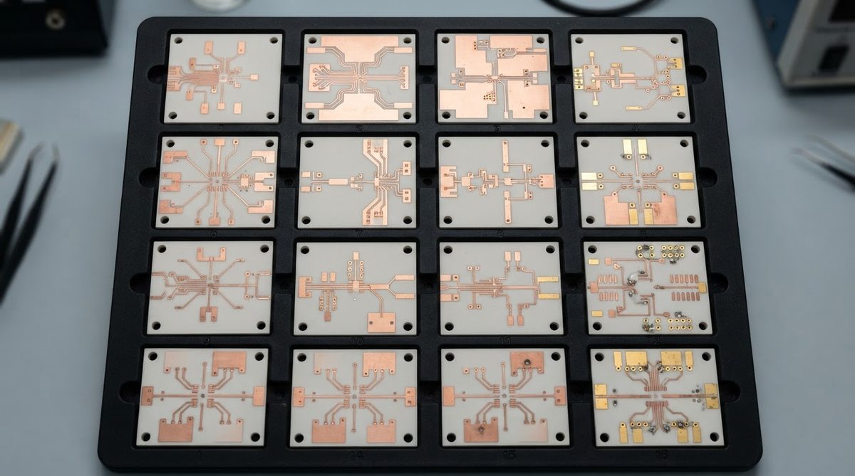
DPC sputters a thin Ti/Cu seed layer onto the alumina, then builds copper thickness by electroplating. Photolithography defines the pattern before or after plating, allowing fine traces down to 30–50 µm. This makes DPC the go-to process for LED thermal substrates, sensor circuits, and RF matching networks where precision matters more than raw current capacity. Both 96% alumina DPC and 99.6% alumina DPC substrates are available depending on thermal requirements.
AMB (Active Metal Brazing)
AMB uses a braze alloy containing an active metal (typically titanium) to chemically bond copper foil to the ceramic at ~850 °C in vacuum. The titanium reacts with Al₂O₃ to form a TiO₂ interface layer, producing the strongest bond of any copper-on-ceramic method. AMB substrates handle the highest thermal cycling stresses and are used in traction inverters, railway power modules, and aerospace converters. Details on alumina-based AMB are on the 96% Al₂O₃ AMB substrate page.
Thick-Film Copper
Screen-printed copper paste (copper particles in a glass-frit binder) is fired at ~850–950 °C in a nitrogen atmosphere to prevent oxidation. The glass frit bonds to the alumina surface. Conductivity is lower than bulk copper (typically 60–80% IACS) because of the glass phase, and the fired layer is thin (10–50 µm). Thick-film copper metallized alumina is cost-effective for resistor networks, heater circuits, and hybrid modules that do not need high current. For comparison with precious-metal alternatives, see gold-metallized ceramic substrates.
Alumina Grade Selection for Copper Metallized Alumina: 96% vs. 99.6%
The alumina purity affects thermal conductivity, surface finish, and cost. Here is a head-to-head comparison relevant to copper metallization.
| Property | 96% Al₂O₃ | 99.6% Al₂O₃ | Unit | Condition | Source |
|---|---|---|---|---|---|
| Thermal conductivity | 24–28 | 28–35 | W/mK | 25 °C, ASTM E1461 | CoorsTek ADS-96, ADS-996 datasheets |
| Dielectric strength | ≥ 8.5 | ≥ 10 | kV/mm | AC, 60 Hz, 25 °C | Kyocera A-493, A-499 datasheets |
| Surface roughness (as-fired) | 0.5–1.0 | 0.2–0.5 | µm Ra | — | Maruwa HA-96, HA-996 |
| CTE | 6.5–7.2 | 6.7–7.4 | ppm/°C | 25–300 °C | CoorsTek datasheets |
| Flexural strength | 350–380 | 400–450 | MPa | 3-pt bend, ASTM C1161 | CoorsTek datasheets |
| Relative substrate cost | 1× | 1.5–2× | — | — | Market pricing |
Typical values for commercially available material, for comparison only. Confirm against the datasheet for your specific grade.
Use 96% alumina for most copper metallized alumina power modules and LED substrates. Move to 99.6% when you need the smoother surface for thin-film DPC patterning below 50 µm line/space, or when the extra thermal conductivity measurably reduces junction temperature in your thermal model.
Worked Example: Thermal Resistance of a DBC Copper-Alumina Stack
Consider a 25 × 25 mm DBC substrate with 0.3 mm copper on both sides and a 0.635 mm 96% alumina core. The die footprint is 10 × 10 mm and dissipates 100 W.
- Copper layer Rth: thickness / (k × area) = 0.0003 m / (390 W/mK × 0.0001 m²) = 0.0077 K/W
- Alumina core Rth: 0.000635 m / (26 W/mK × 0.000625 m²) = 0.039 K/W (using full substrate area for spreading)
- Total substrate Rth (one copper + ceramic + one copper): 0.0077 + 0.039 + 0.0077 ≈ 0.054 K/W
- Temperature rise across the substrate: 100 W × 0.054 K/W = 5.4 °C
This is a simplified 1-D estimate. Lateral spreading in the copper reduces the effective Rth by 15–30% depending on geometry. Use a finite-element tool for production designs, but this back-of-envelope check confirms that the substrate itself contributes only a small fraction of the total junction-to-ambient resistance.
When Not to Use Copper Metallized Alumina
Low power, low frequency, cost-sensitive products. If your board runs under 1 W total and operates below 125 °C, FR-4 or a standard metal-core PCB will cost 5–20× less per unit area. Ceramic is overkill.
Very high thermal conductivity requirements. If 24–35 W/mK through the substrate is not enough—for example, a bare-die GaN HEMT dissipating > 500 W/cm²—consider aluminum nitride (170–200 W/mK) or silicon nitride (80–90 W/mK with superior fracture toughness) instead of alumina.
Large-area boards. Alumina substrates are typically limited to roughly 190 × 140 mm or smaller. If your design exceeds that, you will need tiling or a different substrate technology entirely.
Extreme mechanical shock. Alumina is brittle. A 96% alumina substrate has a fracture toughness of ~3.5 MPa·√m. For applications with repeated mechanical impact, Si₃N₄ (6–7 MPa·√m) is more forgiving.
FAQ
Can you solder directly to copper metallized alumina?
Yes. Copper surfaces accept standard Sn-Ag-Cu (SAC305) solder and high-temperature AuSn or sintered-silver die attach. Apply a surface finish such as ENIG or ENEPIG to prevent copper oxidation before soldering. Bare copper pads will tarnish within days in ambient air.
Does copper oxidize during the DBC bonding process?
The DBC process deliberately uses a controlled oxygen partial pressure to form the Cu₂O bonding layer. After bonding, the outer copper surface carries a thin oxide that is removed by etching during circuit patterning. The finished product ships with clean copper or a protective finish.
What is the maximum operating temperature for copper on alumina?
The copper-alumina bond itself survives well above 600 °C. The practical limit is set by the solder or die-attach material: SAC305 reflows at ~217 °C, AuSn at ~280 °C, sintered silver at 300 °C+. The substrate can operate continuously at 300–400 °C if high-temperature attach methods are used.
Is copper metallization better than silver or gold on alumina?
Copper has the highest electrical and thermal conductivity of the three and costs far less than gold. Silver offers slightly higher conductivity (410 vs. 401 W/mK) but migrates under DC bias and humidity. Gold resists corrosion and is preferred for wire bonding pads, but at 50–80× the metal cost of copper. Most power and thermal substrates use copper for traces and gold only on bond pads.
How thick can copper be on a DPC substrate?
DPC copper is typically 1–200 µm. Thicknesses above 100 µm increase plating time and cost significantly. If you need more than 200 µm, DBC or AMB is a better fit.
Can copper metallized alumina be used for RF circuits?
Yes. 96% alumina has a dielectric constant of ~9.6 and a loss tangent of 0.0001–0.0004 at 1 MHz, making it suitable for microwave circuits up to 40 GHz and beyond. DPC copper with its fine line capability is the preferred metallization for RF transmission lines on alumina.
Next Step
If you have a power module, LED array, or sensor design that needs copper metallized alumina, start by selecting the process (DBC, DPC, or AMB) based on your copper thickness and feature-size requirements. Upload your Gerber files or drawing for a quote—turnaround is typically within 48 hours.