A ceramic heatsink submount is a thin ceramic tile—typically 0.25 mm to 1.0 mm thick—placed directly beneath a semiconductor die to spread heat laterally and conduct it into the package or heatsink below, while electrically isolating the die from the thermal path. Aluminum nitride (AlN) submounts offer 170–200 W/mK thermal conductivity and a CTE of 4.5 ppm/°C that closely matches GaN and SiC die, making them the default choice for high-power laser diodes, RF transistors, and power electronics. Alumina (Al₂O₃) submounts cost roughly one-third as much and work well below 5–10 W per die, while silicon nitride (Si₃N₄) fills the niche where mechanical shock and flexural strength matter more than raw thermal conductivity.
Key Takeaways
- AlN submounts conduct heat 6–8× better than 96% alumina (170–200 W/mK vs. 24–28 W/mK at 20 °C) and closely match the CTE of GaN (3.2 ppm/°C) and SiC (4.0 ppm/°C).
- 96% alumina submounts remain the most cost-effective option for devices dissipating under ~5 W per die, especially when CTE mismatch stress is manageable.
- Si₃N₄ submounts deliver 70–90 W/mK with flexural strength above 700 MPa, suited for automotive power modules subjected to thermal cycling and vibration.
- Submount thickness directly affects thermal resistance: halving the thickness from 0.50 mm to 0.25 mm roughly halves the conduction resistance through the ceramic.
- Metallization quality—whether thin-film TiW/Au, thick-film silver, or DBC copper—often limits thermal and electrical performance more than the ceramic itself.
What Does a Ceramic Heatsink Submount Actually Do?
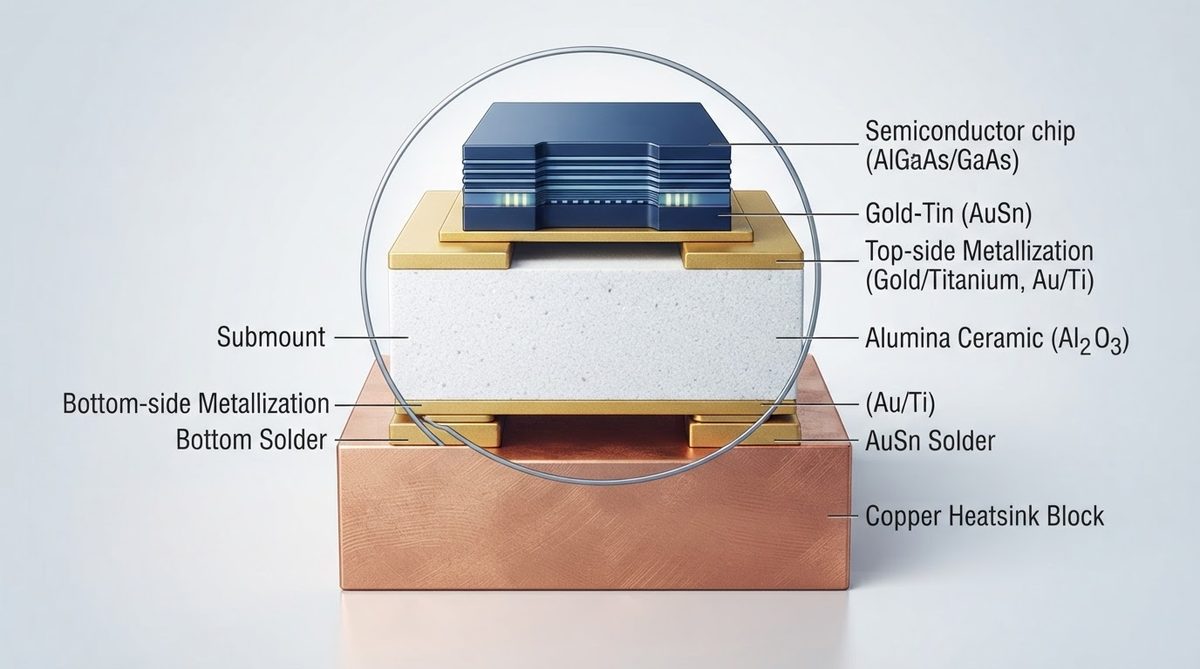
The submount performs three jobs simultaneously. First, it spreads heat from a small die footprint (often under 1 mm²) into a larger area before it reaches the next thermal interface. Second, it electrically isolates the die from a grounded heatsink or package floor, with dielectric strength typically exceeding 10 kV/mm for alumina and AlN. Third, it provides a mechanically stable, solderable platform whose coefficient of thermal expansion (CTE) can be chosen to minimize stress on the die bond during thermal cycling.
In laser diode packaging, for example, a 1 W edge-emitting laser die dissipates its heat through an area as small as 0.3 × 0.5 mm. Without a submount spreading that flux, the thermal resistance from junction to case can exceed 30 °C/W. An AlN submount 0.25 mm thick with gold metallization can reduce that figure to 8–12 °C/W, depending on solder quality and geometry.
Material Comparison: AlN vs. Al₂O₃ vs. Si₃N₄
The table below summarizes the three ceramics most commonly used as heatsink submounts. Each property is given at room temperature unless noted otherwise.
| Parameter | 96% Al₂O₃ | AlN | Si₃N₄ | Unit | Source |
|---|---|---|---|---|---|
| Thermal conductivity (20 °C) | 24–28 | 170–200 | 70–90 | W/mK | Kyocera / CoorsTek datasheets |
| CTE (25–400 °C) | 7.1–7.4 | 4.4–4.7 | 2.7–3.2 | ppm/°C | Kyocera / Maruwa datasheets |
| Dielectric strength | ≥ 10 | ≥ 14 | ≥ 12 | kV/mm | CoorsTek datasheets |
| Flexural strength (ASTM C1161) | 350–380 | 300–350 | 700–850 | MPa | CeramTec / Kyocera datasheets |
| Density | 3.7–3.8 | 3.25–3.30 | 3.2–3.3 | g/cm³ | Maruwa datasheets |
| Relative cost (per cm², unmetallized) | 1× | 3–5× | 4–6× | — | Industry estimate |
Typical values for commercially available material, for comparison only. Confirm against the datasheet for your specific grade.
For a deeper look at grade-specific properties, the ceramic substrate datasheet library collects manufacturer data in one place.
Worked Example: Thermal Resistance Through a Submount
Conduction resistance through a flat submount is straightforward to estimate:
Rth = t / (k × A)
Where t is thickness (m), k is thermal conductivity (W/mK), and A is the effective heat-spreading area (m²). Consider a 5 W laser die on a 3 × 3 mm AlN submount, 0.25 mm thick:
- t = 0.00025 m
- k = 180 W/mK (mid-range AlN)
- A = 9 × 10⁻⁶ m² (simplified, no spreading)
Rth, ceramic = 0.00025 / (180 × 9 × 10⁻⁶) = 0.154 °C/W
Temperature rise through the ceramic alone: 5 W × 0.154 °C/W ≈ 0.77 °C. That is a small fraction of the total junction-to-ambient budget. Compare the same geometry in 96% alumina (k = 26 W/mK): Rth = 1.07 °C/W, ΔT ≈ 5.3 °C. In a laser diode where every degree shifts wavelength by ~0.3 nm, that 4.5 °C difference matters.
Submount thickness options from the ceramic substrate thickness chart range from 0.25 mm to 1.0 mm. Thinner submounts reduce thermal resistance but are harder to handle during die attach and more prone to cracking under clamp loads.
CTE Matching: Why It Drives Material Selection
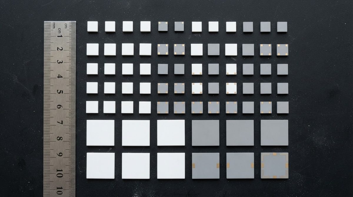
Die attach solder joints fail by fatigue when the die and submount expand at different rates during thermal cycling. The critical metric is the CTE mismatch multiplied by the die size and the temperature swing. GaN-on-SiC die have a CTE around 3.5–4.0 ppm/°C. AlN at 4.5 ppm/°C produces a mismatch of only ~0.5 ppm/°C, resulting in low shear stress across a typical 1 × 1 mm die even over a −40 °C to +150 °C range. Alumina at 7.2 ppm/°C triples that mismatch to ~3.2 ppm/°C, which can crack hard AuSn solder joints within a few hundred thermal cycles on die wider than 2 mm.
Si₃N₄ at 2.8 ppm/°C actually undershoots the CTE of most die materials, but its exceptional flexural strength (700+ MPa per ASTM C1161) lets it absorb the resulting stress without fracturing. This makes it popular in automotive IGBT and SiC MOSFET modules where the substrate endures thousands of power cycles between 25 °C and 175 °C.
Metallization Options for Submounts
The ceramic alone is only half the submount. The metallization stack determines solderability, wire-bondability, electrical resistance, and long-term reliability.
Thin-Film (Sputtered) Metallization
Typical stacks: Ti/Pt/Au or TiW/Ni/Au, with total metal thickness of 0.5–5 µm. Thin film gives the tightest line/space resolution (down to 10–20 µm) and the smoothest surface for eutectic die attach. It is the standard for laser diode and photodetector submounts. Browse alumina 96% thin-film substrates for an example of this process on Al₂O₃.
Thick-Film (Screen-Printed) Metallization
Silver or gold conductor pastes fired at 850 °C, producing 8–15 µm metal layers. Lower cost than thin film, coarser features (minimum ~100 µm line/space), and adequate for power die attach where fine patterning is not needed. Thick-film silver metallized ceramics are a common choice for LED and sensor submounts.
DBC / AMB Copper
Direct bonded copper (DBC) and active metal brazing (AMB) bond 0.15–0.50 mm copper foil to the ceramic. These are overkill for small submounts but become relevant when the submount doubles as a circuit carrier in a power module. AMB on Si₃N₄ is the current standard for high-reliability SiC power modules rated above 200 A.
When NOT to Use a Ceramic Submount
Ceramic submounts add cost and an extra thermal interface. Skip them when:
- Die power is under 0.5 W and CTE mismatch is tolerable. Many small-signal ICs and low-power sensors mount directly on an FR-4 or metal-core PCB with no submount at all.
- The package already provides adequate heat spreading. Copper slugs or integrated heat spreaders inside QFN or TO-247 packages may eliminate the need for a separate ceramic tile.
- Cost is the dominant constraint and thermal margin is generous. An aluminum metal-core PCB (MCPCB) with a dielectric layer of 1–3 W/mK costs a fraction of a ceramic submount and is sufficient for mid-power LEDs.
- Mechanical shock exceeds ceramic limits. In high-g environments (e.g., munitions, downhole tools), a direct solder-on-copper approach with a compliant underfill may survive better than a brittle ceramic interface.
For applications where the ceramic substrate itself serves as the full circuit board bonded to a heatsink, see the guide on mounting a PCB directly on a heatsink.
Frequently Asked Questions
What is the maximum operating temperature of a ceramic submount?
Alumina and AlN submounts themselves remain stable above 1000 °C. The practical limit is set by the metallization and solder: AuSn eutectic melts at 280 °C, and standard thick-film silver conductors are rated to 300–400 °C continuous. Most designs operate well below 200 °C junction temperature.
Can I solder directly to an unmetallized ceramic submount?
No. Bare ceramic is not wettable by solder. You need a metallization layer—thin-film, thick-film, or DBC/AMB copper—to create a solderable surface. Attempting to solder directly to alumina or AlN will produce a non-bonded joint.
How small can a ceramic submount be cut?
Laser-scribed and snapped submounts can be as small as 0.5 × 0.5 mm, though handling becomes difficult below 1 × 1 mm. Tolerances of ±0.05 mm are typical for laser-cut parts. For non-rectangular shapes, custom-shape ceramic substrates can be machined to specific outlines.
Does AlN degrade in humid environments?
Unprotected AlN hydrolyzes slowly in the presence of moisture, forming aluminum hydroxide on the surface. This is rarely a problem inside hermetically sealed packages. For unsealed applications, a passivation layer (SiO₂ or Si₃N₄ thin film) or a conformal coating prevents degradation. Alumina does not have this issue.
What solder is best for die attach on a ceramic submount?
AuSn (80/20) eutectic solder is the industry standard for high-reliability die attach on ceramic submounts. It reflows at 280 °C, forms a void-free joint with proper fluxless processes, and has high creep resistance. SAC305 (SnAgCu) is a lower-cost alternative acceptable for commercial-grade products where the junction temperature stays below 125 °C.