A ceramic chip carrier is a small, flat ceramic substrate designed to mount a bare semiconductor die, provide electrical interconnection, and conduct heat to the next level of packaging. Carriers are made from alumina (Al₂O₃), aluminum nitride (AlN), or occasionally silicon nitride (Si₃N₄), and they bridge the thermal-expansion gap between a silicon or GaAs die and a metal heatsink or PCB below.
Key Takeaways
- 96% alumina chip carriers offer 24–28 W/mK thermal conductivity at 20 °C and a CTE of ~7.1 ppm/°C, close enough to silicon (2.6 ppm/°C) to survive thousands of thermal cycles when die-attach solder is chosen correctly.
- AlN carriers reach 170–200 W/mK with a CTE of ~4.5 ppm/°C, making them the default for high-power laser diodes and GaN HEMTs above 10 W dissipation.
- Leadless ceramic chip carriers (LCCCs) eliminate leads entirely, reducing parasitic inductance to below 1 nH per pad—critical above 10 GHz.
- Metallization choice (gold, silver, or copper) determines solderability, wire-bond pull strength, and long-term reliability in hermetic packages.
What Is a Ceramic Chip Carrier?
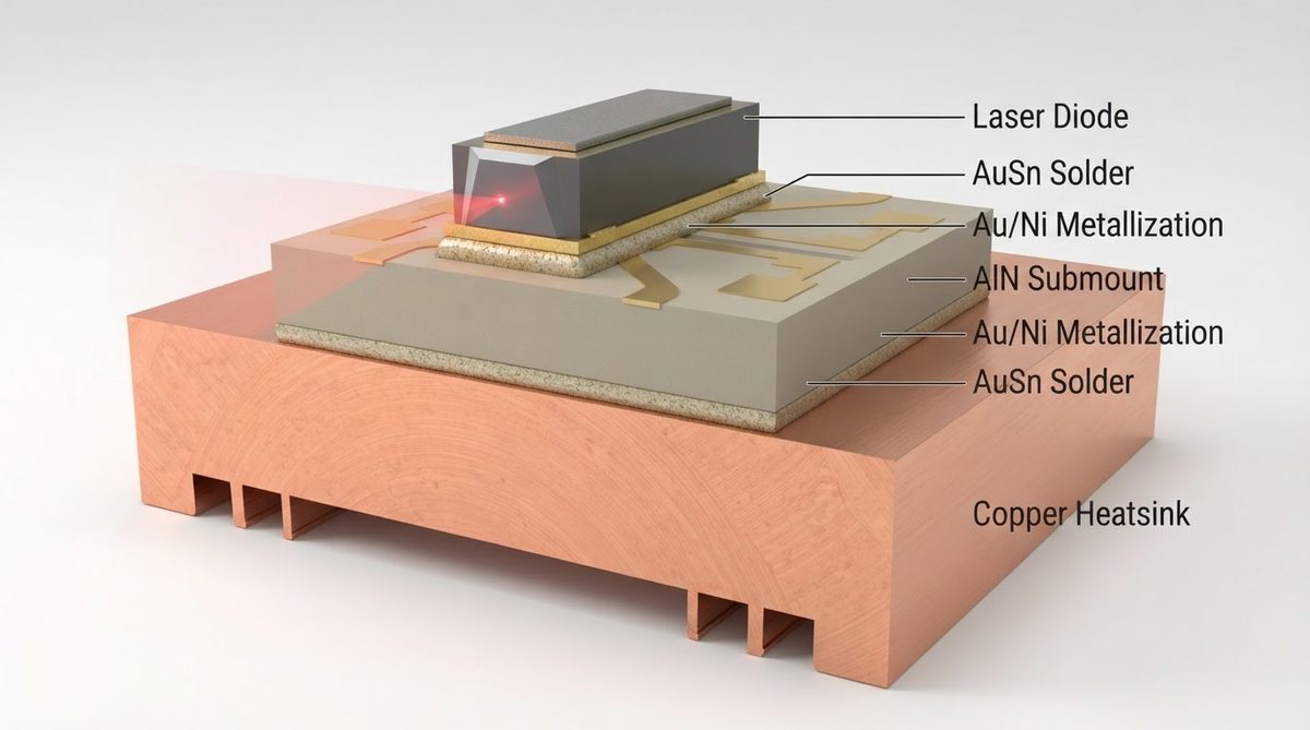
The term covers several related package forms. All share a ceramic body, patterned metallization on one or both faces, and a cavity or flat pad for die placement. The ceramic serves three roles simultaneously: electrical insulator, thermal conductor, and mechanical support.
Common forms include the leaded ceramic chip carrier (CLCC), the leadless ceramic chip carrier (LCCC per JEDEC MS-004), and simple flat submounts with no cavity. Submounts are the simplest variant—a metallized ceramic rectangle that sits between a die and a heatsink, acting as a thermal and CTE buffer. For a deeper look at submount-specific design, see ceramic heat spreaders and submounts.
Material Options for Ceramic Chip Carriers
Material selection is the single most consequential decision. It sets the thermal path, the allowable operating temperature, the CTE match to your die, and roughly 60–70 % of the unit cost.
| Parameter | Al₂O₃ 96% | Al₂O₃ 99.6% | AlN | Unit | Condition |
|---|---|---|---|---|---|
| Thermal conductivity | 24–28 | 28–35 | 170–200 | W/mK | 20 °C, ASTM E1461 |
| CTE | 7.1 | 7.2 | 4.5 | ppm/°C | 20–300 °C |
| Dielectric constant (εᵣ) | 9.4 | 9.9 | 8.8 | — | 1 MHz |
| Flexural strength | 350–380 | 400–450 | 300–350 | MPa | ASTM C1161, 4-pt bend |
| Max continuous use temp. | 1 600 | 1 700 | 1 000 (in N₂) | °C | Oxidation limit in air for AlN ~700 °C |
| Relative cost (Al₂O₃ 96% = 1×) | 1× | 1.3–1.5× | 3–5× | — | Same geometry |
Typical values for commercially available material, for comparison only. Confirm against the datasheet for your specific grade. Sources: CoorsTek ADS-996 datasheet; Maruwa AlN-HP datasheet.
When to pick alumina
96% alumina is the workhorse. It is adequate for die dissipating up to roughly 3–5 W on a 5 × 5 mm carrier, depending on heat-sink quality. It is widely stocked in standard ceramic substrate sizes, and thick-film metallization is straightforward. Choose 99.6% alumina thin-film substrates when you need tighter line/space (below 50 µm) or lower surface roughness for flip-chip bumping.
When to pick AlN
AlN is justified when the thermal path through the carrier dominates junction temperature. A 0.25 mm-thick AlN carrier conducts heat with roughly 6–8× less thermal resistance than the same thickness of 96% alumina. For laser diodes, where wavelength stability depends on junction temperature to within ±1 °C, AlN is effectively mandatory. Explore available options on the AlN thin-film substrate page.
Worked Example: Thermal Resistance Through a Chip Carrier
A 980 nm pump laser die dissipates 4 W. The carrier is 5 mm × 3 mm × 0.25 mm. Compare the conduction resistance (Rth) through the carrier for alumina 96% versus AlN.
Rth = t / (k × A)
For 96% Al₂O₃ (k = 26 W/mK): Rth = 0.00025 / (26 × 0.000015) = 0.64 °C/W → ΔT = 4 W × 0.64 = 2.6 °C
For AlN (k = 180 W/mK): Rth = 0.00025 / (180 × 0.000015) = 0.093 °C/W → ΔT = 4 W × 0.093 = 0.37 °C
The 2.2 °C difference matters for wavelength-critical lasers (roughly 0.3 nm/°C for 980 nm diodes). For a general-purpose IC at the same power, it likely does not.
Metallization and Surface Finish
Bare ceramic cannot be soldered or wire-bonded. The metallization layer defines what assembly processes are possible.
Gold metallization
Thin-film Ti/Pt/Au or TiW/Au stacks are standard for wire bonding and AuSn eutectic die attach. Gold resists oxidation indefinitely, making it the default for hermetic military and space packages. Learn more about gold-metallized ceramic substrates and their specifications.
Silver and copper metallization
Thick-film silver is lower cost and suitable for solder reflow with SnAgCu (SAC) alloys. Copper metallization (via DBC or thick-film firing) provides the best electrical and thermal conductivity but requires a barrier layer (Ni/Au or Ni/Pd/Au) to prevent oxidation and ensure solderability.
Package Styles Compared
| Style | Leads | Cavity | Typical pitch | Best for |
|---|---|---|---|---|
| LCCC (JEDEC MS-004) | None (castellations) | Yes | 1.27 mm (50 mil) | RF, microwave, mil-aero |
| CLCC (J-lead) | J-leads | Yes | 1.27 mm | Socketed test, field replacement |
| Flat submount | None | No | Custom pad layout | Laser diodes, LEDs, sensors |
| CPGA | Pin grid | Yes | 2.54 mm (100 mil) | High-I/O legacy, test sockets |
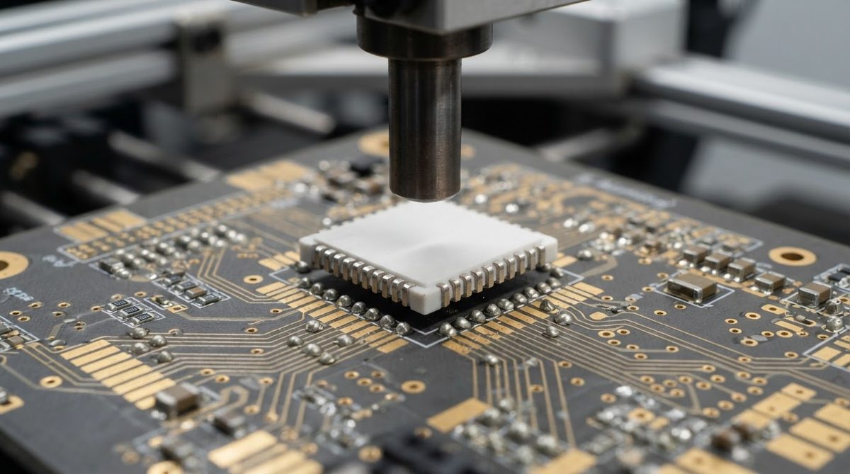
LCCCs dominate RF and microwave packaging because the absence of leads minimizes parasitic inductance. The trade-off is that leadless joints are less compliant under CTE mismatch with an organic motherboard. If the motherboard CTE exceeds ~12 ppm/°C, solder joint fatigue becomes a concern past 500 thermal cycles (per IPC-SM-785 modeling). Column or ball-grid attach can mitigate this.
When NOT to Use a Ceramic Chip Carrier
Cost-driven consumer products. If the die dissipates under 1 W and the operating range is 0–70 °C, a plastic QFN or BGA is 5–20× cheaper and thermally sufficient.
Very high I/O count (> 300 pins). Organic BGA substrates offer finer pitch and more routing layers at lower cost. Ceramic PGA packages exist for high I/O but are heavy, expensive, and limited to 2.54 mm pitch in most standard forms.
Flex or high-vibration environments without mechanical support. Ceramic is brittle. A carrier mounted to a flex circuit or unsupported over a span will crack under shock loads that a polyimide substrate absorbs. Consider a metal-core or flex-rigid alternative.
FAQ
Can I reflow-solder an LCCC to an FR-4 motherboard?
Yes, but CTE mismatch limits reliability. FR-4 expands at 14–17 ppm/°C versus 7 ppm/°C for alumina. For applications requiring more than 500 thermal cycles (–40 to +125 °C), use a CTE-matched carrier board or add compliant solder columns instead of flat pads. IPC-SM-785 provides the fatigue-life calculation method.
What die-attach materials work on a ceramic chip carrier?
AuSn (80/20) eutectic solder is standard for hermetic packages, melting at 280 °C. SAC305 (SnAgCu) works for non-hermetic commercial assemblies. Epoxy die attach (silver-filled) is the lowest-cost option but adds 5–15 °C/W of thermal resistance compared to solder.
How small can a ceramic chip carrier be?
Submounts are routinely produced as small as 0.5 × 0.5 mm with ±25 µm dimensional tolerance using laser scribing. Cavitied LCCCs are practical down to about 3 × 3 mm outer dimension due to wall-thickness limits in cofired alumina.
Does AlN require special handling compared to alumina?
AlN is moisture-sensitive at the surface level. Hydrolysis of exposed AlN in humid environments produces aluminum hydroxide, degrading thermal performance over time. Store AlN carriers in dry nitrogen or vacuum packaging. Metallized surfaces are protected, but exposed edges should be sealed or the package kept hermetic.
Are ceramic chip carriers suitable for space applications?
Yes. Ceramic LCCCs and flat-pack carriers have a decades-long flight heritage. They meet outgassing requirements per ASTM E595 (TML < 1.0%, CVCM < 0.1%) inherently, because fired ceramics contain no volatile organics. Metallization must be tested per MIL-STD-883 for bond strength and hermeticity.
Next Step
If you are evaluating ceramic chip carriers or submounts for a specific die, start by confirming your thermal budget, CTE requirements, and metallization needs. You can request a ceramic substrate sample kit to test die-attach and wire-bond processes on actual material before committing to production quantities.