A laser cut ceramic substrate is a ceramic blank profiled to a custom outline using a focused laser beam—typically CO₂ (10.6 µm), Nd:YAG (1.064 µm), or UV (355 nm)—instead of mechanical scribing, diamond sawing, or waterjet. Laser cutting achieves positional tolerances of ±0.05 mm on most alumina and aluminum nitride grades, with minimal micro-cracking at the kerf edge. This makes the laser cut ceramic substrate the default method for prototype and low-to-mid-volume custom shapes.
Key Takeaways
- A laser cut ceramic substrate holds ±0.05 mm dimensional tolerance on Al₂O₃ (96 % and 99.6 %) and AlN up to roughly 1.0 mm thick.
- Kerf width is typically 0.05–0.15 mm depending on laser type, far narrower than a diamond blade’s 0.2–0.4 mm kerf.
- Edge roughness (Ra) ranges from 1.5 µm to 6 µm, influenced by laser wavelength, pulse rate, and material grade.
- Laser cutting is a non-contact process: no clamping force, no tool wear, and no risk of propagating cracks from mechanical stress.
- For substrates thicker than ~1.5 mm or production runs above ~5,000 pieces, diamond scribing or CNC grinding often wins on cost per part.
Why Laser Cutting Suits Ceramic Substrates
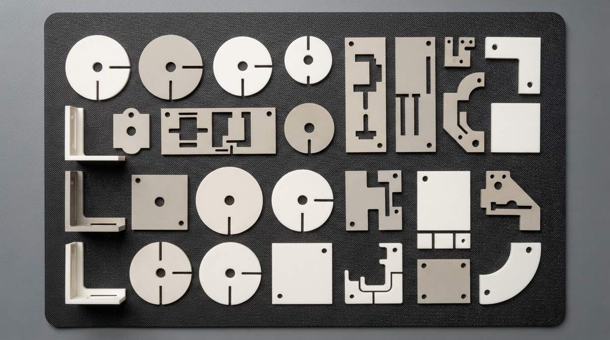
Ceramics are hard and brittle. Mechanical methods—scribing, routing, punching—apply contact force that can initiate micro-cracks at stress concentrators such as inside corners or narrow slots. Laser ablation removes material thermally and photochemically without mechanical load. The result is a clean edge with a heat-affected zone (HAZ) that rarely exceeds 20–50 µm in well-tuned processes.
Because there is no physical tool, complex outlines cost the same as simple rectangles. A substrate with six mounting slots and a curved edge takes the same programming effort as a plain square. This makes laser cutting especially valuable during prototyping, when the outline may change between revisions and hard tooling would be wasteful.
Materials Compatible with a Laser Cut Ceramic Substrate
The table below lists the ceramic materials most commonly laser-cut for electronic substrates, along with the laser types that work well for each.
| Material | Typical thickness range | Preferred laser | Edge Ra (µm) | Notes |
|---|---|---|---|---|
| Al₂O₃ 96 % | 0.25–1.0 mm | CO₂, Nd:YAG | 2–5 | Most common substrate; cuts cleanly at moderate power |
| Al₂O₃ 99.6 % | 0.25–1.0 mm | CO₂, Nd:YAG | 2–4 | Denser grain; slightly smoother edge than 96 % |
| AlN | 0.25–0.635 mm | Nd:YAG, UV (355 nm) | 1.5–4 | Absorbs well at 1.064 µm; avoid excessive heat to limit oxidation |
| Si₃N₄ | 0.32–0.635 mm | UV, Nd:YAG | 3–6 | Toughest ceramic; slower cut speed, higher pulse energy needed |
| ZrO₂ (zirconia) | 0.25–0.5 mm | Nd:YAG, UV | 2–5 | Low thermal conductivity; HAZ slightly wider than alumina |
Typical values for commercially available material, for comparison only. Confirm against the datasheet for your specific grade.
If you need laser-cut alumina parts specifically, Al₂O₃ 96 % is the workhorse grade—widely stocked, lowest cost, and well-characterized for laser processing. For high-power thermal applications, laser-cut aluminum nitride substrates offer thermal conductivity of 170–200 W/mK at 25 °C (per Maruwa and Kyocera datasheets) while still accepting tight-tolerance laser profiling.
Laser Types and How They Differ
CO₂ laser (10.6 µm)
Most oxide ceramics absorb strongly at 10.6 µm, so CO₂ lasers cut alumina efficiently at moderate power (50–200 W). The relatively long wavelength limits minimum feature size to roughly 0.10–0.15 mm. CO₂ is the lowest-cost option for straight cuts and large radii on alumina substrates up to 1.0 mm thick.
Nd:YAG / fiber laser (1.064 µm)
The shorter wavelength delivers a smaller spot size (~30–50 µm), enabling finer features and tighter inside-corner radii. Pulsed Nd:YAG is the standard for AlN because AlN absorbs well at 1.064 µm and the pulsed mode limits thermal input, reducing surface oxidation. Edge quality on alumina is comparable to CO₂ but with a narrower kerf (0.05–0.10 mm).
UV laser (355 nm)
UV lasers ablate ceramic primarily through photochemical bond breaking rather than thermal melting. This produces the smallest HAZ (<10 µm) and the finest features (slots as narrow as 0.05 mm). The trade-off is slow cutting speed and high capital cost, so UV is reserved for thin substrates (≤0.5 mm) requiring very tight geometry—such as ceramic chip carriers with close-tolerance cavity edges.
Tolerances, Kerf, and Edge Quality of a Laser Cut Ceramic Substrate
The three specifications engineers care about most when requesting a laser cut ceramic substrate are dimensional tolerance, kerf width, and edge roughness. Here is what to expect and what drives each one.
| Parameter | Typical range | Primary driver |
|---|---|---|
| Dimensional tolerance | ±0.05 mm (standard), ±0.025 mm (tight) | Stage accuracy, substrate flatness |
| Kerf width | 0.05–0.15 mm | Laser wavelength, beam focus |
| Edge roughness (Ra) | 1.5–6 µm | Pulse rate, material grade |
| Minimum inside-corner radius | 0.10–0.15 mm (CO₂), 0.05 mm (UV) | Spot size |
| Heat-affected zone | 10–50 µm | Pulse duration, thermal conductivity of material |
Values represent well-optimized production processes. Actual results depend on equipment, material lot, and operator settings.
Worked example — kerf compensation. Suppose you need a 10.00 × 10.00 mm laser cut ceramic substrate from 96 % alumina using an Nd:YAG laser with a 0.08 mm kerf. The laser path centerline must be offset outward by half the kerf: 0.04 mm. The programmed cut path is therefore 10.08 × 10.08 mm. After cutting, the finished part measures 10.00 ± 0.05 mm. Forgetting kerf compensation is the most common cause of undersized parts in first-article runs.
Enter your substrate dimensions, material, and laser type below to estimate the temperature rise and derating behaviour at the cut edge during processing.
Design Rules for Laser-Cut Ceramic Parts
These guidelines help you get a clean cut without recuts or scrap. They apply broadly across alumina and AlN; tighten or loosen them based on the specific material and laser type after consulting your supplier.
- Minimum web width: Keep solid material between any two cut edges ≥ 2× the substrate thickness. For a 0.635 mm substrate, that means ≥ 1.27 mm.
- Inside corners: Add a radius of at least 0.10 mm. Sharp 90° inside corners concentrate thermal stress and are the leading cause of micro-cracks.
- Slot width: Minimum 0.10 mm for Nd:YAG, 0.15 mm for CO₂. Narrower slots require UV processing.
- Edge-to-metallization clearance: Keep conductive traces or pads ≥ 0.15 mm from the laser-cut edge. The HAZ can alter dielectric properties in the outermost 20–50 µm.
- Panelization: Leave at least 1.0 mm of sacrificial border around each part for fixturing. Parts can be held in the panel by small breakout tabs (0.3–0.5 mm wide) that snap cleanly after cutting.
- Thickness limit: Laser cutting is practical up to about 1.0–1.5 mm for alumina and 1.0 mm for AlN. Beyond that, multiple passes are needed, widening the kerf and HAZ.
For substrates that combine laser-cut outlines with metallized circuits, it is common to metallize first, then laser-profile. This avoids re-registration issues. If your design calls for gold-metallized ceramic or copper-metallized alumina substrates, discuss the sequence with your supplier early—metallization before cutting is standard, but some thick-film processes require post-fire trimming.
Laser Cutting vs. Other Singulation Methods
| Method | Tolerance | Kerf | Edge quality (Ra) | Thickness limit | Best for |
|---|---|---|---|---|---|
| Laser cutting | ±0.05 mm | 0.05–0.15 mm | 1.5–6 µm | ~1.0–1.5 mm | Prototypes, complex shapes, mid-volume |
| Diamond scribing & break | ±0.10–0.15 mm | ~0.05 mm (scribe line) | 6–15 µm | 0.25–1.0 mm | High-volume rectangles |
| Diamond blade dicing | ±0.025 mm | 0.2–0.4 mm | 0.8–3 µm | Up to 2+ mm | Thick parts, tight tolerance on straight cuts |
| CNC grinding / milling | ±0.01–0.05 mm | N/A (material removed by tool) | 0.4–2 µm | Up to 10+ mm | Thick parts, polished edges, tight geometric tolerances |
| Waterjet | ±0.10–0.20 mm | 0.5–1.0 mm | 3–8 µm | Up to 5+ mm | Thick parts, no HAZ needed |
Values are representative of well-maintained equipment. Source: aggregate of CoorsTek, Kyocera, and Maruwa processing guidelines.
Diamond blade dicing gives a smoother edge and tighter linear tolerance, but it can only cut straight lines. CNC grinding handles any shape and any thickness but is slower and more expensive per part. The laser cut ceramic substrate occupies the middle ground: complex shapes, fast turnaround, and tolerances tight enough for most substrate applications.
Common Applications for Laser Cut Ceramic Substrates
Laser cut ceramic substrates appear wherever a non-rectangular outline or an internal cutout is needed:
- Power module baseplates and spacers — custom outlines to match IGBT or SiC die footprints. Ceramic spacers and washers are a typical example.
- LED submounts — small AlN substrates with tight-tolerance edges for die-attach and wire-bond pads. These often serve as ceramic heat spreaders and submounts.
- RF and microwave housings — alumina lids or frames with internal slots for signal feedthroughs.
- Sensor substrates — thin alumina or zirconia parts with alignment holes and non-standard perimeters for MEMS or gas-sensor packages.
When Not to Use Laser Cutting
Laser cutting is not always the right call. Choose a different method if:
- Your substrate is thicker than 1.5 mm. Multiple laser passes widen the kerf, increase HAZ, and slow throughput. Diamond blade dicing or CNC grinding is more practical.
- You need sub-micron edge finish. Optical or hermetic-sealing applications may require Ra < 1 µm. CNC grinding with a fine-grit diamond wheel achieves this; a laser cut ceramic substrate does not.
- Volume exceeds ~5,000 identical rectangles. Diamond scribing on a panelized sheet is faster and cheaper for simple shapes at scale.
- Zero HAZ is mandatory. Some dielectric or sensor applications cannot tolerate any thermal alteration of the edge zone. Waterjet or CNC grinding avoids thermal effects entirely.
- Your material is very thick Si₃N₄. Silicon nitride’s high toughness (K_IC ~ 5–7 MPa·m^0.5, per CoorsTek data) makes it resistant to ablation. Laser cutting Si₃N₄ above 0.5 mm is slow and may require UV, pushing cost above CNC alternatives.
FAQ
Can you laser-cut a ceramic substrate that already has metallization?
Yes. The standard sequence is to metallize first, then laser-profile. The laser parameters are adjusted so the beam cuts through both the metal layer and the ceramic. Thin-film and thick-film metallizations (Au, Ag, Cu) up to about 20 µm do not significantly affect cut quality. For DBC or AMB substrates with 0.3 mm copper, the copper is typically etched to clear the cut path before laser profiling the ceramic.
Does laser cutting weaken the ceramic?
Flexural strength at the cut edge is slightly lower than at a polished surface—typically 10–20 % reduction—because the HAZ introduces micro-scale thermal stress and grain-boundary changes. For most substrate applications where the edge is not a primary load path, this reduction is irrelevant. If edge strength matters (e.g., a structural spacer under clamping load), post-cut edge grinding restores full strength.
What file format do I need for a laser cut ceramic substrate outline?
DXF is the universal format. Supply the outline as a closed polyline or spline in DXF, with dimensions in millimeters. Gerber files work if the cut outline is on a dedicated board-outline layer. Include a dimensioned PDF drawing as a cross-check.
How fast is laser cutting compared to CNC grinding?
Laser cutting is roughly 5–20× faster in linear cutting speed on substrates ≤ 0.635 mm thick. A 10 × 10 mm alumina part can be profiled in under 10 seconds with an Nd:YAG laser, versus 1–3 minutes on a CNC grinder. The speed advantage narrows as thickness increases.
Is there a minimum order quantity for laser cut ceramic substrates?
Most suppliers, including AluminaPCB, accept orders as low as 1 piece for prototypes. There is no tooling charge because the laser path is defined by a CAD file, not a physical die. This makes laser cutting the lowest-barrier entry point for custom ceramic shapes.
Next Step
If you have a DXF or Gerber outline ready, you can request a quote directly through the custom-shape ceramic machining page to confirm tolerances and lead time for your specific geometry and material. For hands-on evaluation before committing to a production order, consider requesting a ceramic substrate sample kit.