Laser cut aluminum nitride parts combine the high thermal conductivity of AlN (170–200 W/mK at 25 °C, per Maruwa and Kyocera datasheets) with the tight dimensional control that only non-contact cutting can deliver on a brittle ceramic. Typical positional tolerances reach ±25 µm, with kerf widths of 30–80 µm depending on laser source, substrate thickness, and pulse parameters. The result is a finished ceramic part that needs no post-machining for most power-electronics and optoelectronics applications.
Why Laser Cut Aluminum Nitride Instead of Scribe-and-Break
AlN is hard (Vickers hardness ~1,000 HV), brittle, and sensitive to mechanical stress concentrations. Diamond scribing and break—the standard approach for alumina—works on AlN but often produces chipping along the break line. Chips wider than 50 µm can compromise solder pad integrity on an AlN DPC substrate where trace-to-edge clearance may be only 150–200 µm.
Laser ablation avoids mechanical contact entirely. A focused beam vaporises or thermally fractures the ceramic along a programmed path, leaving a clean edge with a heat-affected zone (HAZ) typically under 20 µm for pulsed UV or short-pulse IR lasers. Because the tool never touches the part, there is zero tool wear and no clamping force that could crack thin substrates (0.25–0.38 mm). This is the core reason engineers specify laser cut aluminum nitride for precision thermal components.
Laser Sources Used for Laser Cut Aluminum Nitride
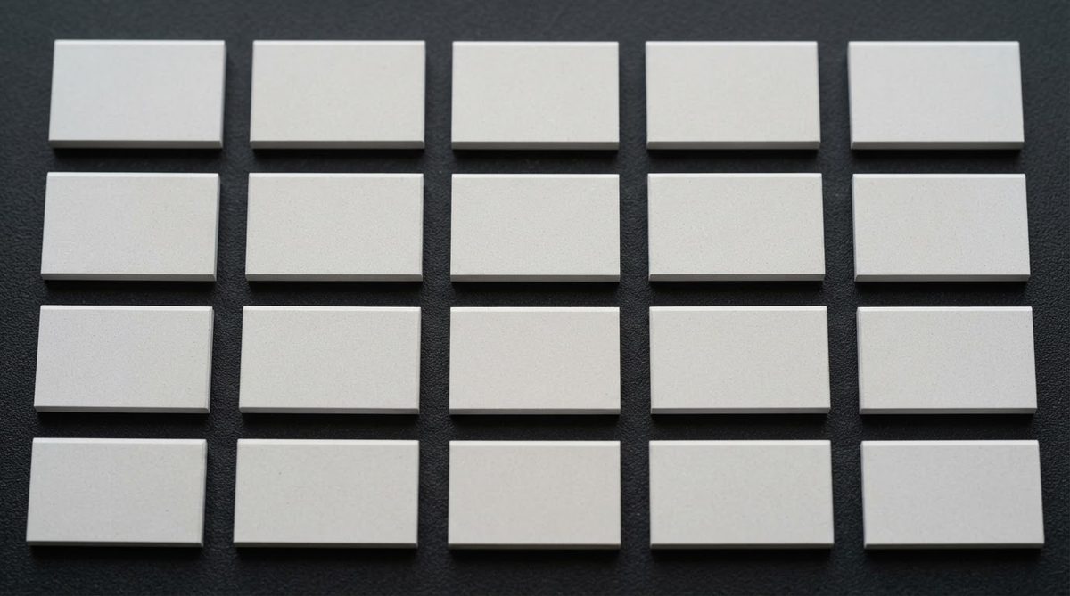
Three laser types dominate AlN processing. The choice depends on required throughput, edge quality, and feature size.
| Laser source | Wavelength | Typical kerf | HAZ | Best for |
|---|---|---|---|---|
| CO₂ (CW / pulsed) | 10.6 µm | 60–100 µm | 30–50 µm | High-speed singulation of thick (≥0.63 mm) substrates |
| Nd:YAG / fibre (pulsed) | 1.064 µm | 40–80 µm | 15–30 µm | General profiling, hole drilling, moderate throughput |
| UV (Nd:YAG 3rd harmonic / excimer) | 355 nm / 248 nm | 20–40 µm | <15 µm | Fine features, tight tolerances, thin substrates |
Typical values for commercially available equipment. Confirm against your laser vendor’s process qualification data for AlN.
CO₂ lasers couple efficiently into AlN because the ceramic absorbs strongly in the far-infrared. Throughput is high, but the wider kerf and larger HAZ limit minimum feature size. UV lasers produce the finest features and smallest HAZ, but at lower cutting speeds—sometimes 5–10× slower than CO₂ for the same thickness. Most production shops use pulsed Nd:YAG or fibre lasers as a practical middle ground for laser cut aluminum nitride work.
Achievable Tolerances and Edge Quality
For a 0.635 mm thick AlN substrate cut with a pulsed 1.064 µm fibre laser, expect these figures:
- Positional accuracy: ±25 µm (referenced to fiducials on the panel)
- Dimensional tolerance: ±50 µm on a 25 × 25 mm part
- Edge roughness (Ra): 3–8 µm, depending on pulse overlap
- Edge chipping: <25 µm with optimised parameters; <10 µm with UV
- Taper angle: 1–3° through-cut; reducible to <1° with multi-pass or dual-side cutting
Compare this with diamond-scribe-and-break on the same material: typical edge chipping of 50–150 µm, positional accuracy of ±100 µm, and no ability to cut curves or internal features. For parts that need slots, notches, or non-rectangular outlines, laser cut aluminum nitride is the only practical option short of diamond grinding—which costs significantly more per part.
Worked Example: Thermal Pad Singulation
A power-module designer needs 200 individual AlN thermal pads, each 12 × 16 mm, cut from a 50.8 × 50.8 mm panel that is 0.38 mm thick. The pads will be bonded to copper via AlN DBC (direct bonded copper) processing after singulation.
Panel yield: A 50.8 mm panel with 80 µm kerf and 0.2 mm inter-part spacing fits 3 columns × 3 rows = 9 parts per panel. That requires 23 panels (23 × 9 = 207 parts, 7 spares).
Cutting time estimate: Each part perimeter = 2 × (12 + 16) = 56 mm. At a pulsed-fibre cutting speed of ~15 mm/s through 0.38 mm AlN, one part takes ~3.7 s of beam-on time. With positioning overhead, assume 5 s per part. One panel of 9 parts: ~45 s. All 23 panels: ~17 min of laser time, excluding load/unload.
This speed makes laser cutting economical even for moderate volumes. Diamond grinding the same 200 parts would require fixturing and typically 30–60 s per part.
Design Rules for Laser-Cut AlN Parts
These guidelines reduce scrap and improve edge quality:
- Minimum internal radius: ≥0.15 mm (limited by kerf width). Specify ≥0.25 mm to stay within standard process windows.
- Minimum slot width: ≥0.15 mm for through-slots; ≥0.25 mm recommended.
- Edge-to-metallisation clearance: ≥0.2 mm. The HAZ can alter surface chemistry near the cut, potentially affecting solder wetting.
- Panel fiducials: Include at least two laser-recognisable fiducials (metallised dots or etched crosses) per panel for registration.
- Thickness uniformity: Specify ±0.025 mm TTV (total thickness variation) on incoming substrates. Thickness variation causes inconsistent cut quality at fixed laser parameters.
For parts that will later receive metallisation via thick-film or thin-film processes, cut before printing whenever possible. Laser debris (recast) on a metallised surface can degrade wire-bond adhesion. If you must cut after metallisation, a post-cut ultrasonic clean in DI water is essential.
Laser-Cut AlN vs. Laser-Cut Alumina
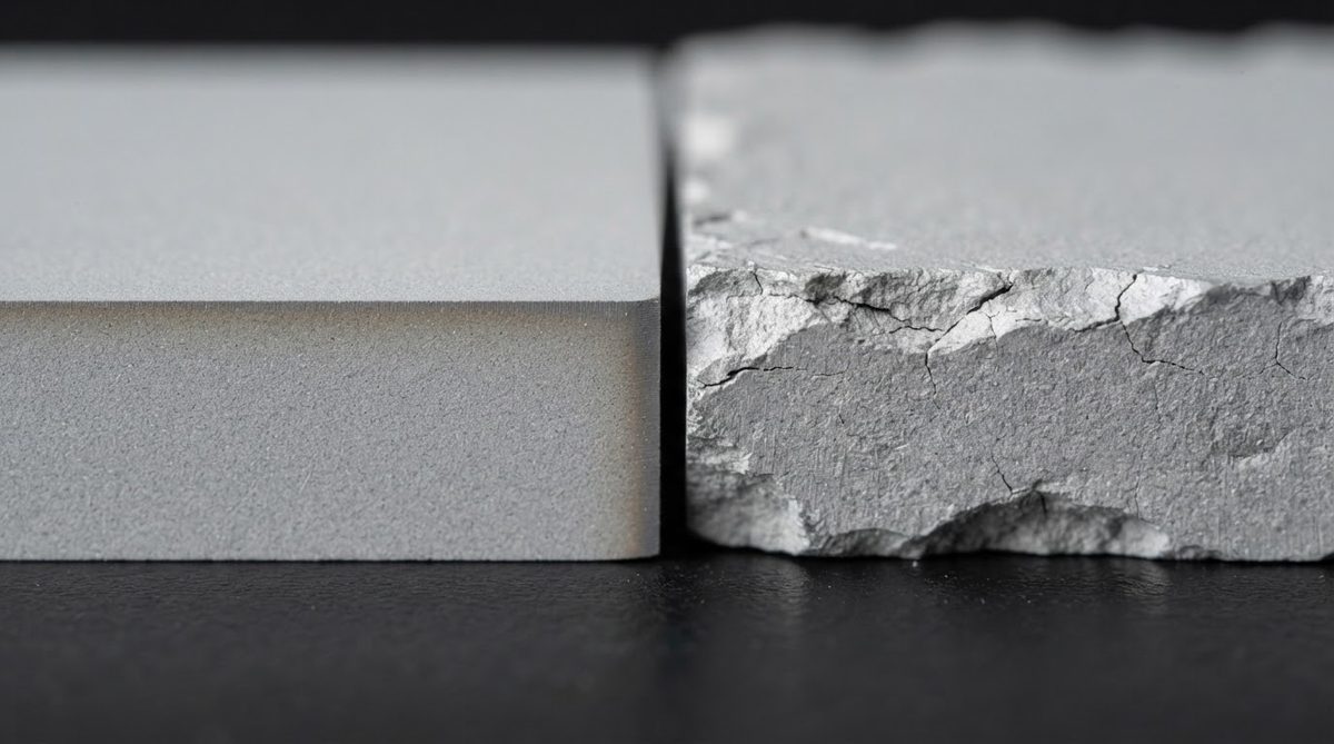
Engineers often ask whether the same laser line that cuts alumina can also handle AlN. The answer is yes, but process parameters differ significantly.
| Parameter | AlN (170–200 W/mK) | Al₂O₃ 96% (24–28 W/mK) | Source |
|---|---|---|---|
| Absorption at 10.6 µm | High | High | CoorsTek material datasheets |
| Absorption at 1.064 µm | Moderate (grey body) | Low (translucent) | Kyocera technical notes |
| Thermal diffusivity | ~80 mm²/s | ~10 mm²/s | Maruwa datasheets, 25 °C |
| Typical cutting speed (1.064 µm, 0.635 mm) | 10–20 mm/s | 15–30 mm/s | Industry process data |
| Edge chipping (optimised) | <25 µm | <30 µm | Industry process data |
Typical values for commercially available material, for comparison only. Confirm against the datasheet for your specific grade.
AlN’s much higher thermal diffusivity means heat spreads away from the cut zone faster, requiring higher peak power to maintain ablation. This is why AlN often cuts slower than alumina at 1.064 µm despite absorbing more of the beam. At 10.6 µm (CO₂), both materials absorb strongly and the speed difference narrows. For a deeper comparison of laser-cut alumina parts, see our dedicated guide.
Applications for Laser Cut Aluminum Nitride Parts
Laser cut aluminum nitride parts appear wherever high thermal conductivity and precise geometry intersect:
- Power electronics: Spacers, heat spreaders, and substrate blanks for DBC and AMB modules. AlN AMB substrates often start as laser-cut blanks before brazing.
- UV-C LED packaging: AlN sub-mounts for 265–280 nm LEDs, where the ceramic also serves as a UV-reflective carrier.
- RF and microwave: Chip carriers and lids where CTE matching to GaN (AlN CTE ~4.5 ppm/°C vs. GaN ~5.6 ppm/°C) reduces die-attach stress.
- Sensor packaging: Hermetic or semi-hermetic housings where precise slot and hole placement is critical.
When Not to Use Laser-Cut AlN
AlN is expensive—roughly 3–5× the cost of 96% alumina per unit area. If your thermal load can be managed with 24–28 W/mK conductivity, alumina is the better economic choice. For parts thicker than ~1.5 mm, laser cutting becomes slow and multi-pass taper grows; diamond grinding or waterjet-assisted cutting may be more practical. And if your geometry is a simple rectangle with generous tolerances (±100 µm or wider), diamond scribe-and-break on AlN is feasible and faster.
For applications where mechanical toughness matters more than thermal conductivity—such as high-vibration automotive inverters—consider silicon nitride AMB substrates instead. Si₃N₄ has roughly 3× the fracture toughness of AlN (≥6 MPa·m⁰·⁵ vs. ~2.5 MPa·m⁰·⁵ per CeramTec data), though its thermal conductivity is lower (70–90 W/mK).
Frequently Asked Questions
Can I laser-cut AlN after metallisation?
Yes, but it adds risk. Laser debris and recast can contaminate solder pads and degrade wire-bond pull strength. If you must cut post-metallisation, use a UV laser to minimise debris and follow with ultrasonic cleaning. Most manufacturers prefer to cut first, then metallise.
Does laser cutting weaken the AlN substrate?
The HAZ introduces micro-cracks that can reduce flexural strength by 10–20% compared to a polished edge, per studies in the Journal of the European Ceramic Society. For structural applications, a post-cut edge polish or anneal restores most of the original strength. For typical die-attach and heat-spreader use, the as-cut strength is adequate.
What file format should I send for laser cut aluminum nitride parts?
DXF or DWG is standard. Include the outline, any internal features, and fiducial locations on separate layers. Gerber files work if the part is a PCB substrate with metallisation, but for bare ceramic profiling, a vector CAD file gives the laser programmer more flexibility.
What is the maximum AlN thickness that can be laser-cut?
Most production laser systems handle AlN up to ~1.0 mm in a single-side cut. Substrates of 1.0–2.0 mm can be cut with multi-pass or dual-side processing, but taper increases and throughput drops. Above 2.0 mm, diamond grinding is usually more practical.
How does laser cutting affect AlN surface roughness near the edge?
Within the HAZ (typically <20 µm from the edge for pulsed IR lasers), surface roughness increases to Ra 5–10 µm. Beyond the HAZ, the original as-fired or lapped surface is unaffected. This is why a 0.2 mm minimum clearance between the cut edge and any metallisation is recommended.