A sputtering seed layer on a ceramic PCB is a vacuum-deposited metal stack—typically 200–500 nm of titanium followed by 500–2,000 nm of copper—that provides the adhesion and electrical conductivity needed for subsequent copper electroplating. The sputtering seed layer ceramic process is essential because copper will not bond reliably to oxide ceramics like Al₂O₃ or AlN without it. Every DPC (direct plated copper) and thin-film metallization process starts here.
Key Takeaways
- The standard sputtering seed layer ceramic stack for DPC is Ti/Cu, deposited in a single vacuum cycle at total thicknesses of 700–2,500 nm.
- Titanium reacts with the ceramic surface to form a TiOx interphase, producing peel strengths of 5–8 N/mm on 96% alumina (per ASTM D3359 cross-hatch testing).
- Seed-layer uniformity across the substrate directly sets the uniformity of the electroplated copper that follows—±5% thickness variation in the seed translates to roughly ±5–8% variation in the final trace.
- Chromium (Cr) and titanium-tungsten (TiW) are alternative adhesion layers, but Ti dominates ceramic PCB production because of its lower cost and simpler etch chemistry.
- Substrate surface roughness (Ra) between 0.2 and 0.8 µm gives the best balance of adhesion and fine-line capability for traces below 50 µm.
What a Sputtering Seed Layer on Ceramic Actually Does
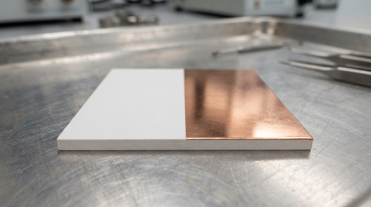
Oxide ceramics are chemically inert. Copper atoms deposited directly onto a polished alumina surface sit on top without forming chemical bonds, and the film peels under mild thermal cycling. A sputtering seed layer on ceramic solves two problems at once: the bottom portion (the adhesion metal) bonds to the ceramic, and the top portion (the conduction metal) provides a low-resistance path for electroplating current.
In a Ti/Cu stack, titanium atoms arrive at the substrate with enough energy (typically 5–15 eV in DC magnetron sputtering) to partially reduce the surface alumina, forming a graded TiOx interphase 2–10 nm thick. This interphase is what actually anchors the metallization. The copper layer on top is too thin to carry circuit current on its own, but it is thick enough to distribute plating current uniformly during the electroplating step that builds the trace to its final thickness—often 5–20 µm for thin-film circuits, or up to 50+ µm for heavy copper on ceramic substrates.
Common Sputtering Seed Layer Ceramic Material Stacks
| Stack | Adhesion layer | Conduction layer | Typical total thickness | Primary use case |
|---|---|---|---|---|
| Ti/Cu | Ti, 200–500 nm | Cu, 500–2,000 nm | 700–2,500 nm | DPC on Al₂O₃ and AlN — most common |
| Cr/Cu | Cr, 30–80 nm | Cu, 500–1,500 nm | 530–1,580 nm | Legacy thin-film hybrids, resistor networks |
| TiW/Cu | TiW (10/90 wt%), 100–300 nm | Cu, 500–1,500 nm | 600–1,800 nm | GaAs and InP RF devices, barrier applications |
| NiCr/Cu | NiCr (80/20), 20–100 nm | Cu, 300–1,000 nm | 320–1,100 nm | Integrated thin-film resistors |
Typical values for commercially available materials, for comparison only. Confirm against the datasheet for your specific grade.
Chromium-based stacks are being phased out in many facilities because of RoHS and REACH restrictions on hexavalent chromium compounds generated during wet etching. Ti/Cu avoids this issue entirely—Ti etches cleanly in dilute HF or peroxide-based chemistries.
Step-by-Step: How the Sputtering Seed Layer Is Deposited on Ceramic
- Substrate cleaning. The ceramic is ultrasonically cleaned in acetone and IPA, then plasma-cleaned (Ar or O₂ plasma, 100–300 W, 5–10 min) inside the sputter chamber to remove adsorbed organics and activate the surface.
- Pump-down. The chamber reaches a base pressure of 1 × 10⁻⁶ Torr or lower. Residual oxygen at this stage degrades adhesion.
- Ti sputtering. Argon is introduced at 2–8 mTorr. A DC magnetron source deposits Ti at 5–15 nm/min. Substrate rotation ensures ±5% uniformity across the panel.
- Cu sputtering. Without breaking vacuum, the Cu target fires at 15–40 nm/min. The Ti/Cu interface stays oxide-free because the substrate never leaves the vacuum.
- Cool-down and unload. The coated substrate cools under vacuum or inert gas before exposure to atmosphere, preventing Cu surface oxidation that would impair photoresist adhesion.
The entire cycle takes 30–90 minutes per batch depending on chamber size and target thickness. For substrates headed into fine-line patterning, consult ceramic thin-film design rules before finalizing seed-layer thickness—thicker seeds are easier to plate but harder to etch cleanly between traces.
How Seed-Layer Thickness Affects Final Trace Quality
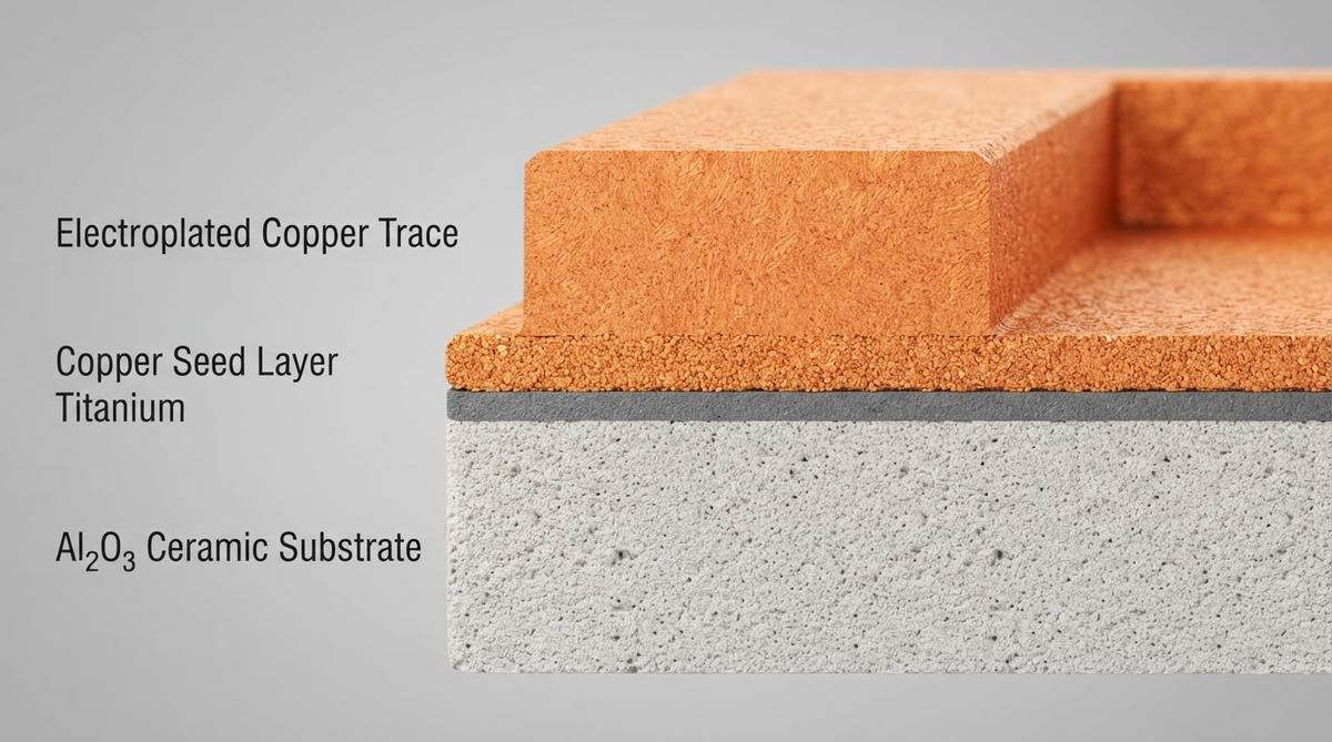
A worked example illustrates the trade-off. Suppose you need 25 µm line / 25 µm space on a 96% alumina substrate with a sputtering seed layer ceramic process.
Scenario A — 300 nm Ti / 800 nm Cu seed (1,100 nm total). After electroplating to 10 µm Cu and photoresist strip, the seed etch removes 800 nm of Cu everywhere. The lateral etch undercut on each side of a 25 µm trace is roughly 0.8–1.2× the seed Cu thickness, so about 0.6–1.0 µm per side. Final trace width lands at approximately 23–24 µm. Acceptable.
Scenario B — 500 nm Ti / 2,000 nm Cu seed (2,500 nm total). Seed etch must remove 2,000 nm of Cu. Lateral undercut per side: 1.6–2.4 µm. Final trace: roughly 20–22 µm, a significant dimensional shift that may violate impedance targets. The thicker Ti layer also requires a longer HF dip, risking attack on exposed ceramic.
The rule of thumb: keep the Cu seed as thin as your plating uniformity allows. For lines below 30 µm, a Cu seed under 1,000 nm is typical. For power circuits where line width tolerance is relaxed, a thicker seed (up to 2,000 nm) reduces plating time and improves current distribution. More detail on plating after the seed step is available at copper plating capabilities and tolerances.
Enter your target trace width, seed-layer Cu thickness, and plating thickness below to estimate lateral undercut and final trace dimensions.
Substrate Material Matters for Sputtering Seed Layer Ceramic Adhesion
The ceramic grade changes how the seed layer behaves. On aluminum nitride thin-film substrates, the native surface is AlN rather than Al₂O₃. Ti still forms a strong bond—TiN forms at the interface instead of TiOx—but AlN is more sensitive to moisture. Substrates must be baked at 150–200 °C for 30+ minutes before loading into the sputter chamber, or trapped water vapor outgasses during deposition and creates voids at the interface.
On 96% alumina, the 4% glassy phase (SiO₂ + CaO + MgO) at grain boundaries can cause localized adhesion variation. Higher-purity 99.6% alumina eliminates most of this glassy phase, giving more consistent peel strength but also a smoother surface that may need deliberate roughening (lapping to Ra 0.3–0.6 µm) for optimal adhesion. For layout considerations specific to thin-film circuits, see thin-film layout guidelines.
When Not to Use a Sputtered Seed Layer
Sputtering is a vacuum batch process. It adds cost and cycle time compared to screen-printed thick-film metallization. If your design can tolerate 100 µm line/space or wider, a thick-film metallization process is simpler, cheaper, and sufficient. Thick-film pastes bond to the ceramic through a glass frit mechanism that needs no vacuum equipment at all.
DBC (direct bonded copper) and AMB (active metal brazing) also skip the seed layer entirely—they bond bulk copper foil to the ceramic in a furnace. These processes suit power modules that need 150–300 µm copper but do not need fine traces. If your minimum feature is above 200 µm and your copper is above 100 µm, DBC or AMB will usually be more cost-effective than sputtering plus plating.
For prototypes that only need a few traces, laser-patterned thick film may be faster to turn around than a sputtered thin-film process.
Frequently Asked Questions
Can I use gold instead of copper for the seed conduction layer?
Yes, Au seed layers are used in wire-bondable thin-film circuits, typically as Ti/Pt/Au or Ti/Ni/Au stacks. Gold seeds cost significantly more and are reserved for applications where wire-bond reliability or corrosion resistance in harsh environments justifies the expense.
Does the sputtering seed layer affect high-frequency performance on ceramic?
The Ti adhesion layer is lossy at GHz frequencies because titanium has high resistivity (~42 µΩ·cm). At 10 GHz and above, a 500 nm Ti layer can measurably increase insertion loss. Designers targeting mmWave often specify a thinner Ti layer (100–200 nm) or switch to TiW, which allows a thinner adhesion film while maintaining peel strength.
How do I inspect seed-layer quality before plating?
Sheet resistance measurement with a four-point probe is the fastest check. A 1,000 nm Cu seed should read roughly 17–20 mΩ/sq. Values above 25 mΩ/sq suggest the film is too thin, oxidized, or poorly nucleated. Peel testing per ASTM D3359 on a witness coupon from the same batch confirms adhesion.
What happens if the seed layer is too thin?
Below about 400 nm total Cu, the seed may not form a continuous film—it can be islanded. Electroplating current then concentrates at connected islands, causing rough, nodular deposits and open circuits between them. A minimum of 500 nm Cu seed is a practical lower bound for most DPC processes.
Is sputtering the only way to deposit a seed layer on ceramic?
E-beam evaporation also works and is common in research labs. It produces less substrate heating but poorer step coverage on rough surfaces. Ion-beam-assisted deposition (IBAD) improves adhesion further but at higher equipment cost. For volume ceramic PCB production, DC magnetron sputtering dominates because of its throughput and uniformity.