Screen printing ceramic substrates is the primary method for depositing conductive, resistive, and dielectric pastes in thick-film PCB production. It reliably places 10–25 µm wet-film deposits that fire into 8–15 µm dried traces, with line widths typically ranging from 100 µm to 250 µm depending on mesh count and paste rheology. The process is mature, cost-effective for medium-to-high volumes, and compatible with alumina (Al₂O₃ 96% and 99.6%), aluminum nitride (AlN), and zirconia (ZrO₂) substrates.
Key Takeaways
- Standard screen printing ceramic achieves 100–125 µm minimum line/space on 96% alumina using 325-mesh stainless steel screens.
- Common conductor pastes are silver (Ag), gold (Au), silver-palladium (AgPd), and tungsten (W, for co-fired ceramics).
- Fired film thickness lands between 8 µm and 15 µm for conductors and 15–40 µm for dielectrics, per DuPont and Heraeus datasheets.
- Post-print firing at 850 °C (thick-film air-fire) or 1,500–1,600 °C (co-fire HTCC) fuses the paste to the substrate.
- Screen printing cannot match thin-film resolution; if you need traces below 50 µm, switch to sputtering or DPC.
How Screen Printing Ceramic Substrates Works
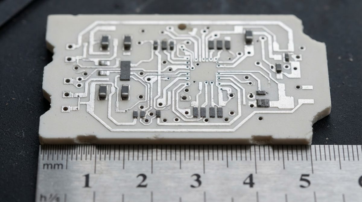
A patterned stainless-steel or polyester mesh screen is stretched over a frame. Paste is placed on the screen, and a squeegee forces it through the open mesh areas onto the ceramic substrate below. The substrate sits on a vacuum chuck to prevent movement. After printing, the wet film goes through a drying oven (100–150 °C, 10–15 min) to drive off solvents, then through a belt furnace for final firing.
Each functional layer—conductor, resistor, dielectric, or overglaze—requires a separate screen and a separate print-dry-fire cycle. A typical thick-film hybrid with two conductor layers and one resistor layer therefore passes through the printer at least three times. Registration between prints is held to ±25–50 µm on modern semi-automatic printers, tightening to ±10–15 µm on fully automatic systems with vision alignment.
Paste Types and Their Roles in Screen Printing Ceramic Circuits
| Paste type | Common materials | Sheet resistance (fired) | Typical use | Source |
|---|---|---|---|---|
| Conductor | Ag, Au, AgPd, AgPt | 2–20 mΩ/□ | Traces, pads, ground planes | Heraeus C8729 / DuPont 6145 |
| Resistor | RuO₂-based, BiRuO₃ | 10 Ω/□ – 1 MΩ/□ | Embedded resistors, trimmable | DuPont 2000 series |
| Dielectric | Glass-ceramic composites | — | Crossover insulation, capacitor layers | Heraeus IP series |
| Overglaze | Lead-free glass | — | Passivation, environmental protection | ESL 4771-G |
Typical values for commercially available material, for comparison only. Confirm against the datasheet for your specific grade.
For co-fired processes (HTCC), tungsten (W) or molybdenum-manganese (MoMn) pastes replace noble metals because they survive the 1,500–1,600 °C sintering temperatures used in co-fired ceramics. These refractory metal pastes have higher sheet resistance (roughly 8–15 mΩ/□) than silver but are essential for multilayer builds where conductor and ceramic must densify together.
Screen Selection: Mesh Count, Wire Diameter, and Emulsion
The screen mesh count directly controls minimum feature size and deposit thickness when screen printing ceramic. A 325-mesh screen (325 wires per inch, ~28 µm wire diameter) is the standard starting point for fine-line thick-film work. Moving to 400 mesh tightens resolution to about 75–100 µm line/space but reduces paste transfer volume, yielding thinner fired films.
Emulsion thickness above the mesh (EOM) adds another control variable. Thicker EOM (15–25 µm over mesh) increases deposit height for power conductors, while thinner EOM (5–10 µm) improves edge definition. For detailed rules on trace geometry and spacing, see the thick-film ceramic design rules.
Worked Example: Estimating Wet Deposit Thickness
Wet deposit thickness ≈ (mesh opening² × EOM) / (mesh opening + wire diameter)². For a 325-mesh screen with 45 µm openings, 28 µm wire, and 15 µm EOM:
T_wet ≈ (45² × 15) / (45 + 28)² = (2,025 × 15) / 5,329 ≈ 5.7 µm from mesh transfer, plus the 15 µm EOM contribution. In practice, total wet deposit lands around 18–25 µm, drying and firing down to 10–14 µm. These numbers align with Heraeus application note AN-TF-001 for standard conductor prints.
Firing Profiles and Substrate Compatibility
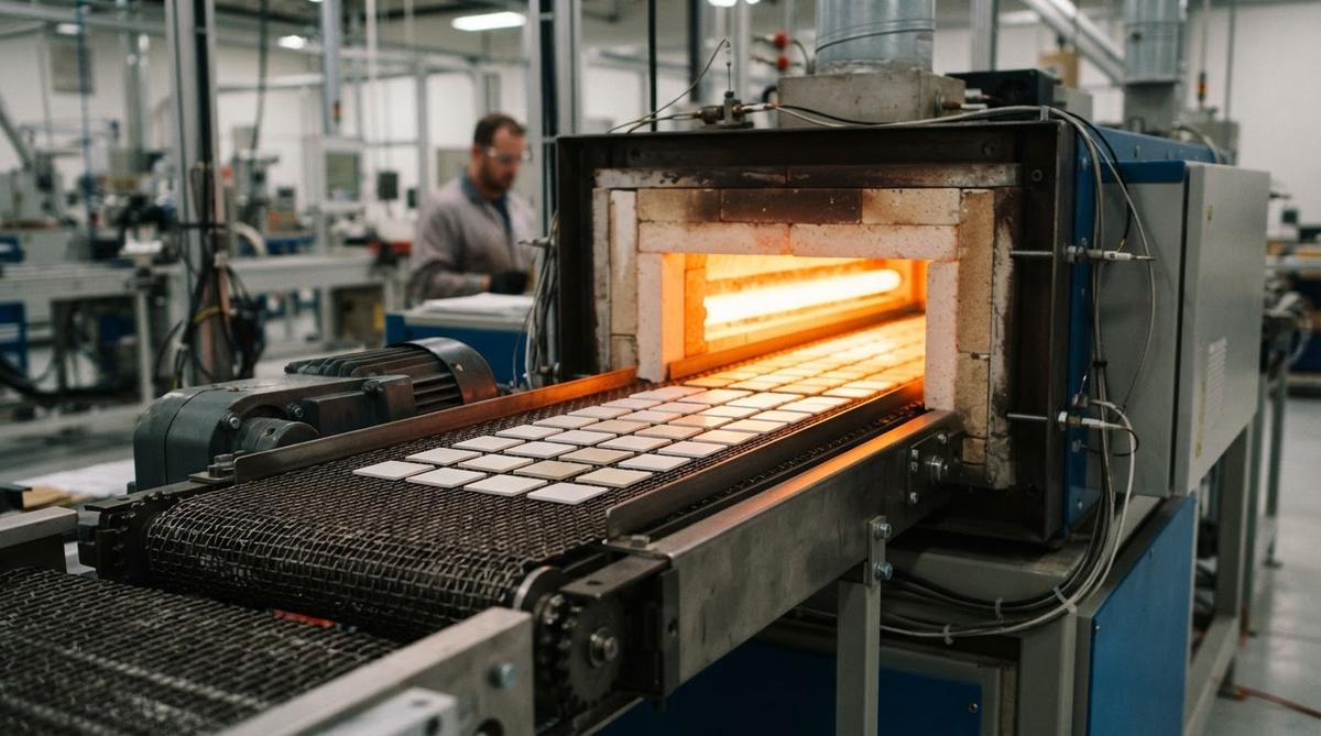
Post-print thick-film firing follows a belt-furnace profile: ramp to 850 °C peak over 10 min, hold at peak for 8–12 min, cool over 20 min. Total cycle is roughly 45–60 min. The peak temperature must remain below the substrate’s safe operating limit. Alumina 96% handles continuous service at 1,600 °C and tolerates repeated 850 °C firing cycles without degradation. AlN substrates also survive these temperatures, though AlN requires a nitrogen or forming-gas atmosphere to prevent surface oxidation above 700 °C in air.
For information on what temperatures ceramic substrates can tolerate in service, see ceramic PCB maximum temperature ratings.
Print Tolerances and What Drives Them
| Parameter | Standard capability | Fine-line capability | Unit | Condition |
|---|---|---|---|---|
| Minimum line width | 150 | 100 | µm | 325-mesh, Ag paste |
| Minimum space | 150 | 100 | µm | 325-mesh, Ag paste |
| Fired thickness (conductor) | 10–15 | 8–12 | µm | Single print |
| Thickness tolerance | ±2 | ±1.5 | µm | Within panel |
| Registration (layer-to-layer) | ±50 | ±15 | µm | Auto vs. semi-auto printer |
| Positional accuracy | ±25 | ±10 | µm | Vision-aligned printer |
Typical values for commercially available material, for comparison only. Confirm against the datasheet for your specific grade.
The biggest yield killers are mesh clogging (from dried paste in open areas), snap-off distance drift, and squeegee pressure variation. Cleaning the screen every 20–50 prints and controlling ambient humidity between 40–60% RH keeps defects in check.
Screen Printing vs. Thin-Film Patterning
Screen printing ceramic and thin-film patterning (sputtering plus photolithography) serve different resolution tiers. If your design calls for traces below 75 µm or impedance-controlled RF lines with tight width tolerance (±3 µm), screen printing cannot deliver. Thin-film processes such as sputtered seed-layer metallization achieve 10–25 µm line/space but cost significantly more per panel due to vacuum deposition and photoresist steps.
For most power electronics, LED substrates, heater circuits, and sensor platforms, the 100–250 µm resolution of screen printing ceramic is sufficient and far more economical. Choose the process that matches your actual feature requirements, not the finest one available.
When NOT to Use Screen Printing on Ceramic
- Traces below 75 µm. Thin-film or DPC processes are required.
- Tight impedance control for RF. Screen-printed conductor width tolerance of ±15–25 µm makes controlled impedance unreliable above a few GHz. Consider thin-film layout approaches covered in thin-film layout guidelines.
- Very thick copper (>35 µm). Screen printing deposits 8–15 µm per pass. Multiple prints can build up to ~40 µm but with diminishing edge quality. Electroplated or DBC copper is better for high-current paths.
- High-volume single-layer circuits on FR-4. If the substrate does not need to be ceramic (no extreme temperature, no high thermal conductivity, no hermeticity), an FR-4 or metal-core PCB will cost a fraction of a thick-film ceramic board.
Frequently Asked Questions
Can screen printing deposit copper paste on ceramic?
Yes, but copper pastes require nitrogen-atmosphere firing to prevent oxidation, which adds process cost. Silver and gold pastes dominate thick-film ceramic work because they fire in air at 850 °C. Copper paste is used mainly when cost-per-gram of noble metals is prohibitive and the production line supports inert-atmosphere furnaces.
How many layers can you screen print on a ceramic substrate?
Practical thick-film builds reach 3–5 conductor layers with interleaved dielectric prints. Each layer adds a print-dry-fire cycle, so cost and cycle time scale roughly linearly. For builds beyond 5 layers, co-fired HTCC or LTCC multilayer processes are more efficient.
Does screen printing ceramic work on aluminum nitride?
Yes. AlN substrates accept standard thick-film pastes, but firing must occur in a nitrogen or forming-gas atmosphere to prevent AlN surface oxidation. Some paste suppliers (Heraeus, DuPont) offer AlN-specific formulations with glass frits designed to bond to the nitride surface.
What is the typical cost per print pass?
A single screen-print pass on a 4.5″ × 4.5″ alumina panel costs roughly $0.50–$2.00 in volume (1,000+ panels), including paste material, screen amortisation, and furnace time. Paste cost is the dominant variable: gold paste at $80–$120/g versus silver paste at $3–$6/g changes the economics dramatically.
How long does a screen last before replacement?
A stainless-steel mesh screen typically survives 5,000–15,000 impressions before mesh fatigue or emulsion wear degrades print quality. Polyester screens are cheaper but last only 1,000–3,000 impressions. Inspect screens under magnification every 500 prints to catch early mesh damage.
Next Step
If you are designing a thick-film ceramic circuit, start with the thick-film layout guidelines to set your line widths, pad sizes, and clearances before generating Gerber files. When your design is ready for quoting, upload it at AluminaPCB’s instant quote page to get pricing and lead times.