LTCC co-fired ceramic design rules center on managing shrinkage, via registration, and conductor resolution across a multilayer stack fired at 850–900 °C. Minimum line/space is typically 100–125 µm with standard screen printing, vias start at 100–150 µm diameter, and X-Y shrinkage tolerance of ±0.1–0.3% after firing must be designed in from the start. Getting these numbers wrong causes open vias, shorted conductors, or warped substrates that cannot be reworked.
Key Takeaways
- Standard LTCC line/space is 100–125 µm; finer features (down to 50 µm) require photoimageable pastes or specialized screens.
- Via diameters range from 100 µm to 300 µm; aspect ratios above 1:1 risk incomplete fill and open circuits after firing.
- X-Y shrinkage during co-firing is 12–16% (material-dependent), with a post-fire tolerance of ±0.1–0.3% achievable with zero-shrinkage or constrained-sintering techniques.
- Layer counts of 10–40+ are routine; each tape layer is typically 50–250 µm green (unfired) thickness.
- Conductor materials are limited to those compatible with the 850–900 °C firing profile: silver, gold, and silver-palladium alloys.
What Is LTCC and How Does It Differ from HTCC?
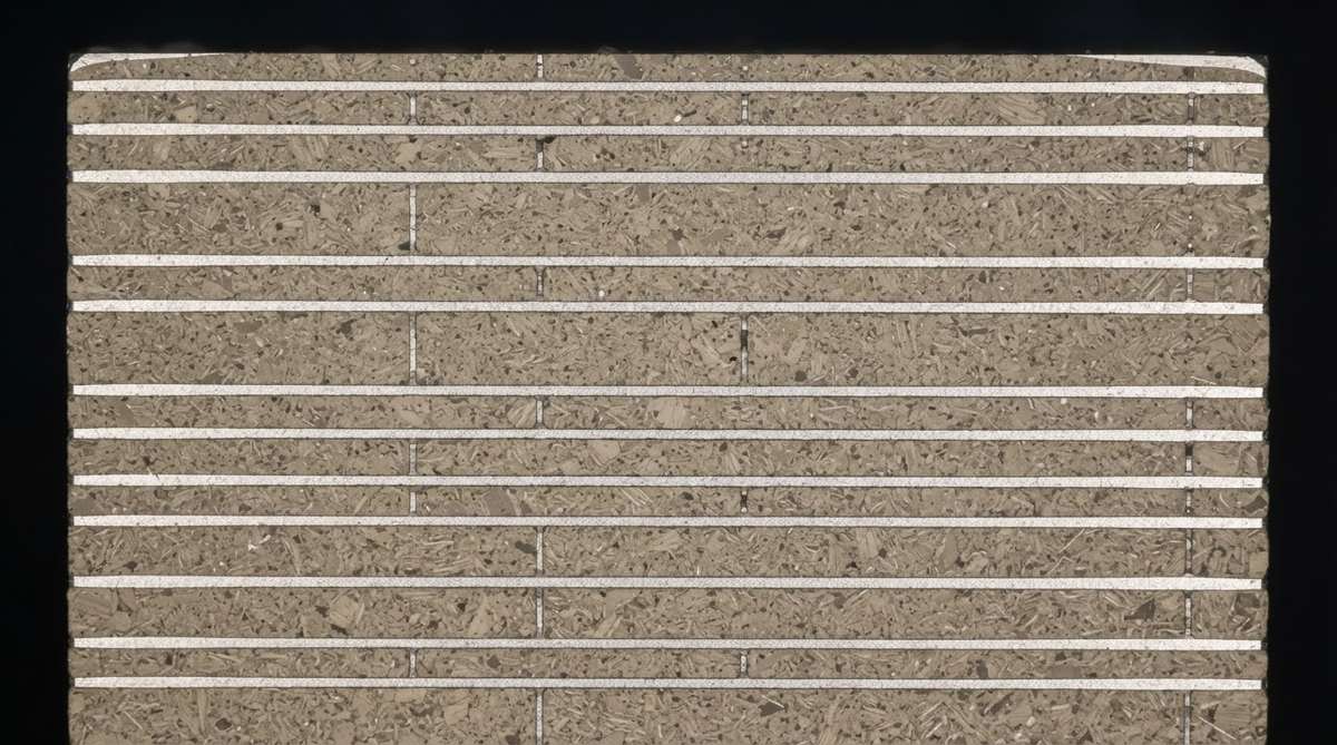
LTCC (Low-Temperature Co-fired Ceramic) is a multilayer ceramic fabrication process in which glass-ceramic green tapes are patterned, stacked, laminated, and co-fired in a single step below 950 °C. The low firing temperature allows the use of high-conductivity metals like silver (σ ≈ 6.3 × 10⁷ S/m) and gold instead of the refractory tungsten or molybdenum required by HTCC (fired at 1,400–1,600 °C).
This distinction drives most of the design-rule differences. Silver conductors have lower resistivity, enabling narrower traces for a given current, but silver migration under DC bias and humidity must be managed through spacing rules. The glass-ceramic tape systems (e.g., DuPont 951, Ferro A6M) each have their own shrinkage profile and dielectric constant, so design rules are partly material-specific. Always confirm shrinkage data against the tape manufacturer’s datasheet.
LTCC Co-fired Ceramic Design Rules: Critical Dimensions
| Parameter | Typical Range | Unit | Condition / Notes | Source |
|---|---|---|---|---|
| Min line width | 100–125 | µm | Standard screen print; 50 µm with photoimageable paste | DuPont 951 Design Guide |
| Min line space | 100–125 | µm | Ag conductors; increase to 150 µm for DC bias >50 V to limit Ag migration | DuPont 951 Design Guide |
| Via diameter | 100–300 | µm | Punched or laser-drilled; 150 µm most common | Ferro A6M datasheet |
| Via pad diameter | Via + 100–150 | µm | Annular ring ≥50 µm per side for registration | Industry practice |
| Via aspect ratio (depth:diameter) | ≤1:1 | — | Higher ratios risk incomplete paste fill | IMST GmbH LTCC guidelines |
| Green tape thickness | 50–250 | µm | Per layer; thinner tapes improve via fill but increase handling risk | DuPont / Ferro datasheets |
| Fired layer thickness | 40–200 | µm | After ~15% Z-shrinkage | DuPont 951 Design Guide |
| X-Y shrinkage | 12.7 ± 0.1–0.3 | % | DuPont 951; zero-shrinkage tapes hold ±0.05% | DuPont 951 datasheet |
| Z shrinkage | 15 ± 0.5 | % | DuPont 951 | DuPont 951 datasheet |
| Layer-to-layer registration | ±25–50 | µm | Optical alignment with fiducials | Industry practice |
| Max layer count | 40+ | layers | Limited by lamination pressure uniformity and co-fire warpage | VTT Technical Research Centre |
| Dielectric constant (εr) | 7.1–7.8 | — | At 1 MHz, 25 °C; DuPont 951 | DuPont 951 datasheet |
| Loss tangent (tan δ) | 0.001–0.006 | — | At 1–10 GHz; material-dependent | DuPont / Ferro datasheets |
Typical values for commercially available material, for comparison only. Confirm against the datasheet for your specific grade.
Shrinkage Compensation: The Core LTCC Design Challenge
Every feature in an LTCC design must be scaled to account for shrinkage during firing. If the tape system shrinks 12.7% in X-Y, a 10.000 mm feature on the fired part must be drawn at 10.000 / (1 − 0.127) = 11.455 mm on the green tape artwork. This sounds straightforward, but the tolerance band matters more than the nominal shrinkage.
A ±0.3% X-Y tolerance on a 50 mm panel means the final dimension could land anywhere in a 50 ± 0.15 mm window. For a BGA land pattern with 0.5 mm pitch, that 150 µm uncertainty consumes most of your pad-to-pad alignment budget. Constrained-sintering (zero-shrinkage) LTCC tapes reduce X-Y shrinkage tolerance to ±0.05%, but they push all shrinkage into the Z-axis, which thickens the substrate and changes impedance. Pick your trade-off early.
Worked Example: Shrinkage-Scaled Via Pad
Target fired via pad diameter: 300 µm. Tape system: DuPont 951, X-Y shrinkage = 12.7%.
Green-state pad diameter = 300 / (1 − 0.127) = 343.7 µm → round to 345 µm on artwork.
With ±0.3% tolerance, the fired pad could be 300 ± (345 × 0.003) ≈ 300 ± 1.0 µm. For the pad itself this is fine, but if the via hole is 150 µm and shrinkage runs high, the annular ring on one side could thin to ~70 µm. Design your annular ring budget to survive the worst-case tolerance stack.
Conductor and Via Fill Rules
LTCC conductors are applied by screen printing on ceramic green tape using thick-film pastes. Fired conductor thickness is typically 8–15 µm for signal layers and up to 25 µm for ground planes. Thicker prints require multiple passes and increase the risk of tape deformation during lamination.
Vias are punched or laser-drilled in the green tape, then filled with conductive paste (usually silver). Incomplete fill is the most common LTCC defect. To avoid it, keep the via aspect ratio at or below 1:1. For a 100 µm tape, that means a minimum via diameter of 100 µm. If your stackup uses 200 µm tape layers, use 200 µm or larger vias. Stacked vias across multiple layers are standard, but stagger them by at least one via diameter if the layer-to-layer registration budget is tight.
For designs that require finer conductors or tighter tolerances than screen printing allows, compare thin-film ceramic design rules, which achieve 10–25 µm line/space through photolithographic patterning on a fired substrate.
Embedded Passives and Cavities
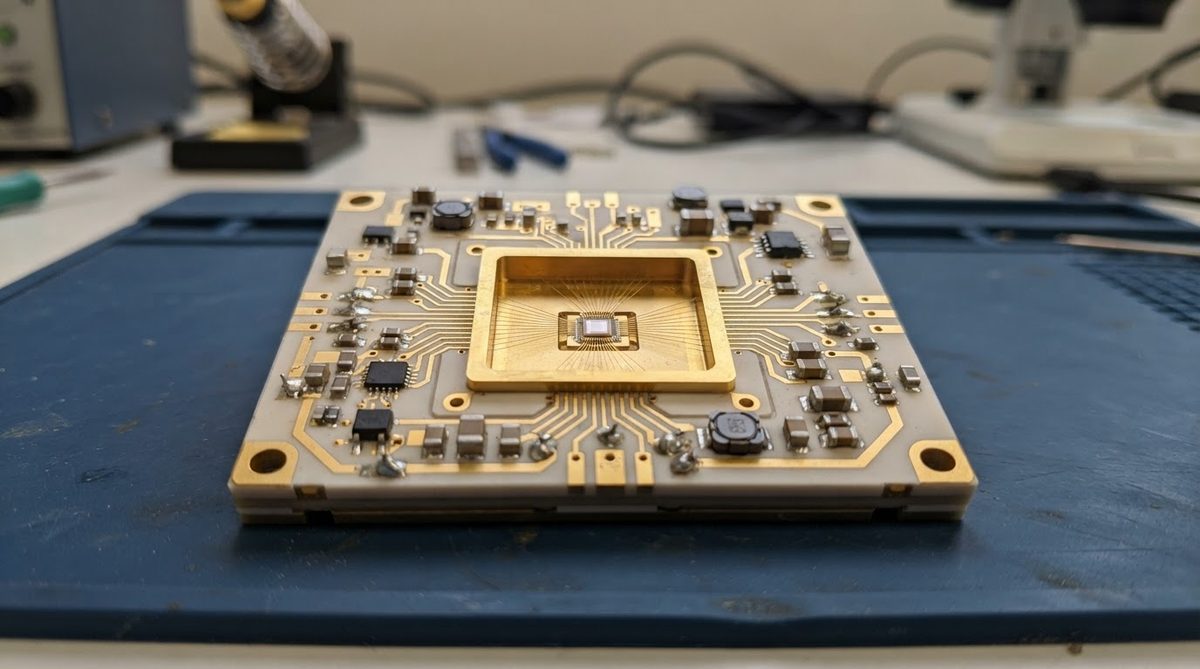
LTCC’s ability to embed resistors, capacitors, and inductors within the ceramic stack is one of its primary advantages over organic PCBs. Embedded resistors use resistive pastes (e.g., ruthenium oxide) printed between conductor layers; typical sheet resistance ranges are 10 Ω/□ to 100 kΩ/□. Tolerance on as-fired embedded resistors is ±20–30%, so laser trimming after firing is standard for precision circuits.
Cavities for bare-die attach or sensor windows are formed by omitting tape layers or cutting windows before lamination. Cavity depth tolerance depends on tape thickness tolerance (typically ±5–8% per layer). For cavity-down designs, maintain a minimum wall thickness of 2× the tape layer thickness to prevent cracking during lamination or firing. Detailed LTCC layout guidelines for cavities and keepouts will save revision cycles.
Design Rules for RF and High-Frequency LTCC
LTCC is widely used for RF modules, filters, and antenna-in-package designs up to 77 GHz and beyond. At RF frequencies, conductor surface roughness, dielectric tolerance, and via parasitics dominate performance.
Stripline impedance in LTCC depends on the fired dielectric thickness and εr. For a 50 Ω stripline in DuPont 951 (εr ≈ 7.4), a signal trace width of roughly 85 µm with a ground-to-ground spacing of 200 µm (two 100 µm layers) is a starting point. Run a 2.5-D field solver with the actual fired dimensions and tolerance bands before finalizing. Via fences for ground shielding should use via-to-via spacing ≤ λ/20 at the highest operating frequency to suppress parallel-plate modes.
When Not to Use LTCC
LTCC is the wrong choice if your design needs only one or two layers. The process overhead of tape casting, punching, lamination, and co-firing makes single- or double-sided boards far more expensive per unit area than thick-film ceramic circuits printed on a pre-fired alumina substrate.
If your operating temperature stays below 150 °C and your frequency is under 3 GHz, a high-Tg FR-4 or Rogers laminate will cost a fraction of LTCC with adequate performance. LTCC also cannot carry heavy copper (>25 µm fired) for high-current power buses; for that, consider thick copper on ceramic via DBC or active metal brazing.
Silver migration is a real concern in high-humidity, high-voltage DC applications. If your bias exceeds 100 V DC in a humid environment, gold conductors or hermetic sealing add significant cost.
FAQ
Can I use copper conductors in LTCC?
Not with standard LTCC tapes fired in air. Copper oxidizes at 850–900 °C in an oxygen-containing atmosphere. Some nitrogen-fireable LTCC systems exist (e.g., Heraeus CT2000), but they are less common, more expensive, and the tape selection is limited. Most LTCC designs use silver or gold.
How tight can layer-to-layer registration get in LTCC?
±25 µm is achievable with optical fiducial alignment on modern LTCC fabrication lines. Production environments typically guarantee ±50 µm. This sets the minimum annular ring and overlap rules for your via pads and conductor-to-conductor alignment.
What is the maximum number of layers in an LTCC stack?
Stacks of 40 or more layers have been demonstrated in production. The practical limit is set by lamination pressure uniformity and co-fire warpage, not by the process itself. Above 20 layers, simulate the thermo-mechanical stress profile and plan for intermediate lamination steps.
Does LTCC require a cleanroom?
Tape blanking, via punching, and screen printing are typically done in a controlled environment (Class 10,000 / ISO 7 or better) to prevent particulate contamination between layers. Full cleanroom conditions (Class 1,000 or better) are used for RF and fine-line LTCC to avoid print defects.
How do I specify LTCC tolerances on my drawing?
Call out post-fire (sintered) dimensions, not green-state dimensions. The fabricator scales artwork to compensate for shrinkage. Specify positional tolerances for critical features (via locations, cavity edges, pad centers) as ± values referenced to a datum, and note the tape system by name so the fabricator can apply the correct shrinkage factor.
Next Step
If you have a multilayer ceramic design in progress, review your via aspect ratios and shrinkage budget against the rules above before submitting files. For a detailed look at metallization capabilities and tolerances, visit the linked page. When you are ready for a design review or quote, submit your files through the instant quote page.