Laser marking is the most reliable way to place permanent part numbers, lot codes, date stamps, and 2D barcodes on ceramic PCBs. Unlike ink printing, a laser mark is fused into or ablated from the substrate surface, so it survives soldering, cleaning, and continuous operation above 300 °C without fading or flaking.
Key Takeaways
- Nd:YAG (1064 nm) and CO₂ (10.6 µm) lasers are the two workhorses for PCB laser marking on ceramic substrates.
- Mark line widths of 30–80 µm are typical on Al₂O₃ 96%; AlN requires lower power density to avoid micro-cracking.
- Laser marks add zero thickness, so they do not interfere with wire bonding, die attach, or lid sealing.
- Keep marks at least 0.5 mm from conductor edges and at least 1.0 mm from bonding pads to avoid thermal damage to metallization.
How Laser Marking Works on Ceramics
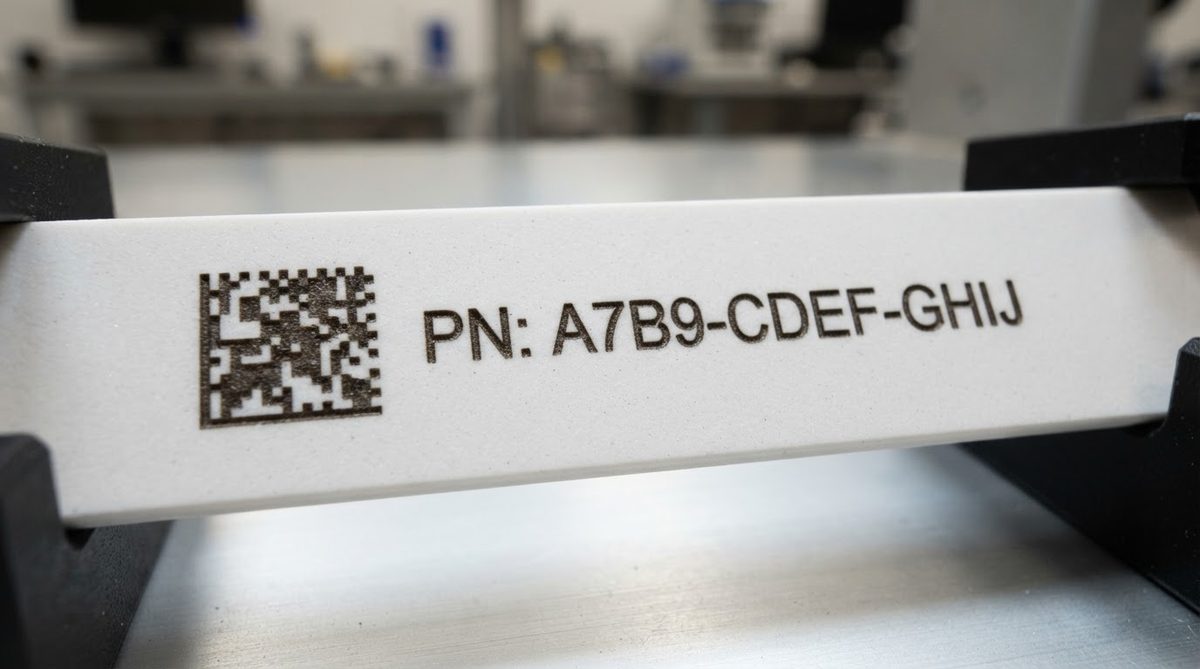
A focused laser beam heats a small area of the ceramic surface past its ablation or colour-change threshold. On alumina, the beam removes a thin layer (typically 5–20 µm deep), creating a visible contrast between the marked and unmarked regions. On aluminum nitride, the mechanism is partly oxidation: the laser converts a shallow surface zone from grey AlN to white Al₂O₃, producing a light-on-dark contrast without significant material removal.
Because the mark is a physical change in the substrate, it cannot be rubbed off, dissolved by solvents, or degraded by UV exposure. This makes laser marking the default choice for automotive, aerospace, and medical traceability requirements per IPC-1066 (Marking and Labeling of Components).
Laser Types and Parameter Selection
Two laser sources dominate ceramic PCB marking. The choice depends on substrate material, required resolution, and throughput.
| Parameter | Nd:YAG / Fiber (1064 nm) | CO₂ (10.6 µm) |
|---|---|---|
| Best suited for | Al₂O₃, AlN, Si₃N₄ | Al₂O₃ (96% and 99.6%) |
| Typical spot size | 20–50 µm | 80–150 µm |
| Achievable line width | 30–60 µm | 80–200 µm |
| Mark depth (Al₂O₃ 96%) | 5–15 µm | 10–30 µm |
| Throughput (characters/s) | 50–200 | 20–80 |
| Risk on AlN | Low at ≤ 8 W avg | Micro-cracking above 15 W avg |
| 2D barcode capable | Yes (Data Matrix down to 2 × 2 mm) | Marginal at small sizes |
Typical values for commonly available industrial marking systems, for comparison only. Confirm against the laser manufacturer’s application note for your specific substrate grade.
Fiber lasers (a modern variant of Nd:YAG) have largely replaced lamp-pumped YAG systems because they offer better beam quality (M² < 1.3), longer diode life, and lower maintenance. For most ceramic PCB work, a 10–20 W fiber laser with a galvo scan head provides the best balance of resolution and speed.
Design Rules for Mark Placement
Where you put the mark matters as much as how you make it. Poorly placed marks can damage conductors, weaken the substrate at a stress riser, or become unreadable after assembly.
- Clearance from conductors: Maintain ≥ 0.5 mm from the nearest trace or pad edge. The heat-affected zone around a laser mark extends 50–150 µm into the substrate, which can degrade adhesion of adjacent ceramic metallization if the clearance is too tight.
- Clearance from wire-bond pads: ≥ 1.0 mm. Micro-debris from ablation can contaminate bond surfaces.
- Avoid score lines and edges: Keep marks ≥ 0.8 mm from scribed or laser-cut edges. Ablation grooves at a substrate edge act as crack initiation sites.
- Mark on bare ceramic, not on metallization: Marking over screen-printed thick-film conductors is possible but reduces conductor thickness locally and can compromise current-carrying capacity. Mark on unmetallized zones whenever layout permits.
- Orientation: Specify mark orientation in your Gerber or DXF package. Most fabs default to reading direction parallel to the longest substrate edge.
Marking on Different Ceramic Materials
Al₂O₃ (96% and 99.6%)
White alumina provides strong contrast with ablation marks, which appear as a matte grey groove. Both fiber and CO₂ lasers work well. Higher-purity 99.6% alumina is slightly harder (Vickers HV 1500–1700 vs. 1200–1400 for 96%), so expect 10–15% slower marking speed at the same depth.
AlN
Aluminum nitride is more thermally sensitive. Excessive pulse energy causes radial micro-cracks visible under 50× magnification. Use short pulses (< 100 ns), low average power (≤ 8 W for a 50 µm spot), and a high repetition rate to build contrast through multiple passes rather than a single deep cut. The resulting white-on-grey mark is highly readable.
Si₃N₄
Silicon nitride is the toughest common ceramic substrate (fracture toughness 5–7 MPa·√m per CeramTec data). It tolerates aggressive marking parameters, but its dark colour means contrast comes from surface roughness rather than colour change. A shallow, wide mark (100 µm line width) with oblique lighting reads better than a narrow, deep one.
Worked Example: Data Matrix Barcode on a 25 × 25 mm DPC Substrate
A power module design requires a 16 × 16 module Data Matrix code encoding a 20-character lot string. Minimum cell size per ISO/IEC 16022 for reliable scanning is 125 µm. That gives a code footprint of 16 × 0.125 = 2.0 mm per side. A 10 W fiber laser at 80 kHz repetition rate, 60 ns pulse width, and 800 mm/s scan speed marks each cell in roughly 1.5 µs. Total marking time for the full code: approximately 0.4 s. Add 1.5 s for the alphanumeric part number (12 characters, 1.5 mm cap height). The entire marking cycle finishes in under 2 s per board, well within typical production takt times.
For substrates processed through copper plating or sputtered seed layers, laser marking is performed after all wet-process steps to prevent chemical attack on the mark surface.
When Not to Use Laser Marking
Laser marking is overkill—or the wrong tool—in several situations:
- Prototype runs under 10 boards: Hand-written or adhesive labels may suffice if traceability requirements are informal.
- Marks on thick-film resistors: Laser trimming and laser marking use the same equipment family, but marking over a resistor element changes its value. Use ink-jet or pad printing if the only available real estate overlaps a resistor zone.
- Flexible or organic substrates: CO₂ lasers char FR-4 and polyimide rather than producing a clean mark. UV lasers (355 nm) are better for organics, but that is a different process entirely.
- Large-area graphics or logos: For cosmetic marks covering more than ~50 mm², screen printing ceramic with a fired ink is faster and cheaper.
Frequently Asked Questions
Does laser marking weaken the ceramic substrate?
A properly parameterized mark removes only 5–20 µm of material and does not measurably reduce flexural strength per ASTM C1161 three-point bend testing. Over-powered marks that gouge deeper than 50 µm can act as stress risers, so always validate parameters on sample coupons before production.
Can laser marks survive reflow soldering?
Yes. Because the mark is an ablation or oxidation feature in the ceramic itself, it is unaffected by lead-free reflow profiles up to 260 °C peak or even high-temperature soldering at 350 °C+. Contrast and readability remain unchanged.
Is laser marking done before or after metallization?
After all metallization, plating, and surface-finish steps. Marking before wet processing risks chemical contamination of the mark groove, which reduces contrast. The one exception is HTCC or LTCC substrates, where marks can be co-fired into the green tape before sintering.
What is the smallest readable text on a ceramic PCB?
With a fiber laser, characters at 0.5 mm cap height are reliably readable under 5× magnification. For automated optical inspection (AOI) readability, 1.0 mm cap height is a practical minimum. Data Matrix codes can go down to 2 × 2 mm footprint with 125 µm cells.
Does mark colour vary between ceramic grades?
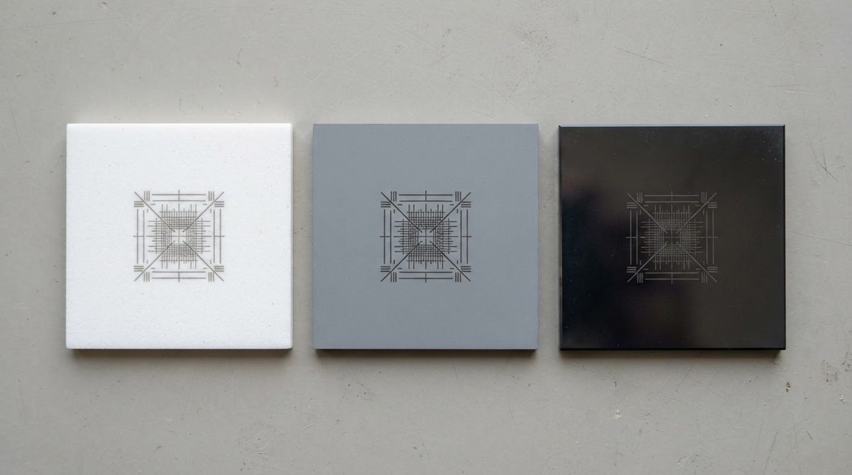
Yes. On white Al₂O₃, marks appear grey to dark brown. On grey AlN, marks appear white due to surface oxidation. On dark Si₃N₄, marks appear lighter grey. Contrast depends on surface roughness, laser wavelength, and viewing angle.
Next Step
If your design requires part-number marking, include the mark location, content string, and barcode type in your fabrication drawing. For a quote on ceramic PCBs with laser-marked traceability, request a quote from AluminaPCB and attach your drawing package.