Lapping grinding ceramic substrate processes are three distinct material-removal methods used to control thickness, flatness, and surface roughness of fired ceramic blanks. Lapping with free abrasive typically achieves Ra 0.1–0.4 µm on alumina; grinding with a bonded diamond wheel is faster but leaves Ra 0.4–0.8 µm; polishing with sub-micron slurry can push Ra below 0.02 µm. Choosing the right lapping grinding ceramic substrate sequence depends on your flatness tolerance, metallization method, and cost target.
- Grinding removes material fastest (5–50 µm per pass) and sets gross thickness, but leaves subsurface damage that can weaken thin substrates.
- Lapping uses loose abrasive between a flat plate and the substrate, delivering flatness under 5 µm across 50 mm and Ra 0.1–0.4 µm.
- Polishing with colloidal silica or diamond slurry (0.25–1 µm grit) achieves mirror finishes below Ra 0.02 µm, critical for thin-film metallization.
- Surface roughness directly affects adhesion of sputtered or evaporated metal layers: thin-film processes generally require Ra ≤ 0.05 µm, while thick-film screen printing works fine at Ra 0.4–0.8 µm.
- Over-polishing adds cost without benefit—specify only the finish your metallization actually needs.
How Lapping and Grinding of a Ceramic Substrate Differ from Polishing
All three processes remove ceramic material, but they do it with different mechanics and leave different surface signatures.
Grinding uses a rigid wheel embedded with diamond abrasive (typically 20–80 µm grit), spinning at high speed against the substrate. It is the fastest way to bring a fired ceramic blank to target thickness. The trade-off is subsurface microcracking. In 96% Al₂O₃, grinding-induced cracks can extend 10–30 µm below the finished surface (per Marinescu et al., Handbook of Ceramics Grinding and Polishing, 2nd ed., Elsevier). For substrates thinner than 0.25 mm, this damage layer is a meaningful fraction of total thickness and can reduce flexural strength by 20–40% versus a lapped surface.
Lapping uses loose abrasive—usually boron carbide, silicon carbide, or diamond—suspended in a slurry between a cast-iron or ceramic plate and the workpiece. The plate rotates slowly, and the abrasive rolls and slides rather than cutting in fixed tracks. This produces a matte, uniformly scratched surface with much less subsurface damage than grinding. Lapping is the standard finishing step for substrates destined for thick-film screen printing or DBC bonding.
Polishing replaces mechanical fracture with a combination of fine mechanical abrasion and chemical attack (chemo-mechanical polishing, or CMP). A polyurethane pad loaded with colloidal silica (particle size 20–80 nm) produces a specular surface. This is essential for thin-film circuit deposition, where a single scratch taller than the metal layer (often 0.1–1 µm) creates an open circuit.
Typical Surface Roughness and Flatness by Lapping Grinding Ceramic Substrate Process
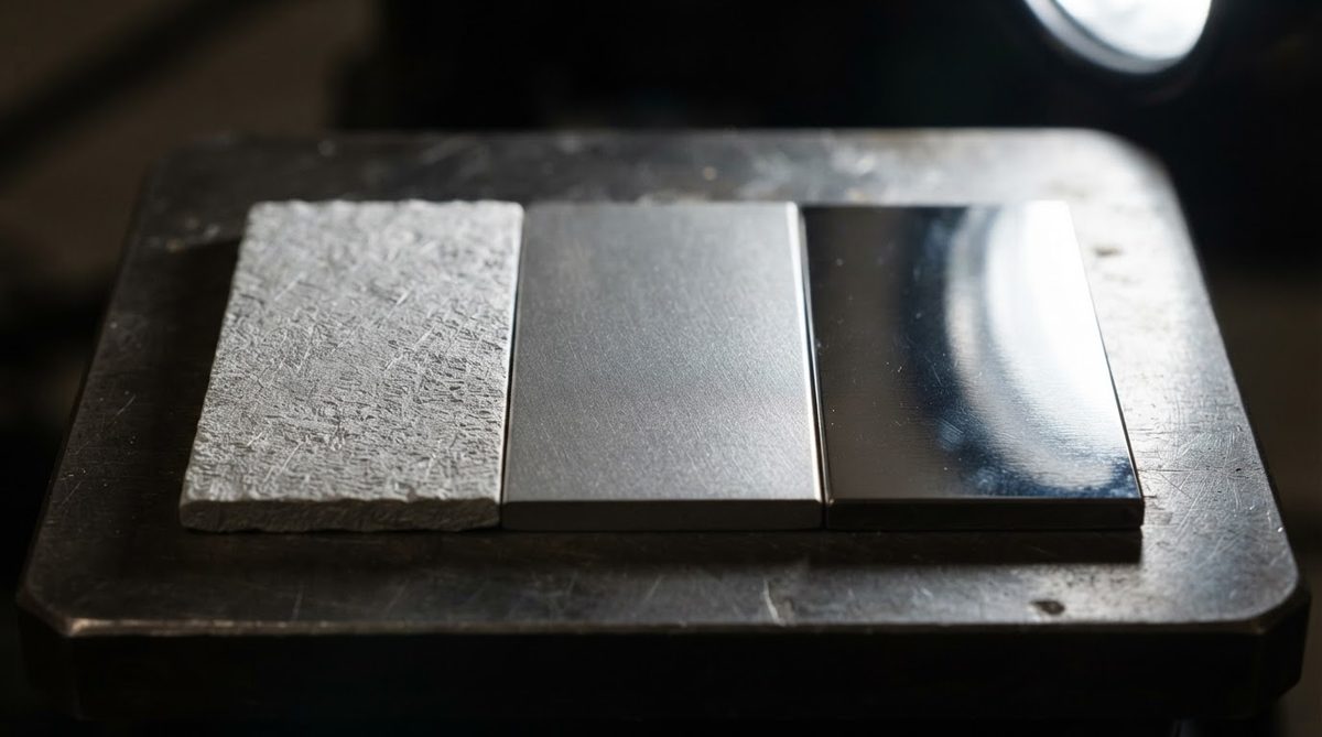
| Parameter | Grinding | Lapping | Polishing | Unit | Condition |
|---|---|---|---|---|---|
| Surface roughness (Ra) | 0.4–0.8 | 0.1–0.4 | 0.005–0.05 | µm | Measured per ISO 4287 |
| Flatness (TTV over 50 mm) | 10–25 | 2–5 | 1–3 | µm | Measured per ASTM F1530 |
| Typical material removal rate (Al₂O₃ 96%) | 5–50 | 1–5 | 0.1–0.5 | µm/min | Varies with pressure and grit |
| Subsurface damage depth (Al₂O₃ 96%) | 10–30 | 2–8 | <1 | µm | Per Marinescu, Elsevier 2015 |
Typical values for commercially available material, for comparison only. Confirm against the datasheet for your specific grade.
Choosing the Right Lapping Grinding Ceramic Substrate Sequence
Most ceramic substrates do not need all three steps. The decision tree is simple: start from your metallization method and work backward.
Thick-film circuits (screen-printed conductors, resistors): Grind to thickness, then lap to Ra 0.2–0.6 µm. Thick-film pastes actually bond better to a slightly rough surface because the glass frit in the paste flows into micro-valleys during firing. A mirror polish here wastes money and can reduce adhesion. See thick-film design rules for paste-specific recommendations.
Thin-film circuits (sputtered Ti/Cu, TaN, NiCr): Grind, lap, then polish to Ra ≤ 0.05 µm. Sputtered metal layers conform to the substrate topography. If Ra exceeds the film thickness, you get discontinuous coverage and unreliable traces. For AlN substrates, CMP with alkaline colloidal silica is preferred because AlN reacts with water; acidic slurries cause pitting.
DBC / AMB bonding: Lap to Ra 0.2–0.4 µm and flatness ≤ 5 µm TTV. The copper-ceramic bond in DBC relies on a eutectic oxide layer, not mechanical keying, so a very smooth surface is unnecessary. But flatness matters: a warped substrate traps gas pockets under the copper foil, creating voids that increase thermal resistance.
Enter your substrate material, target Ra, and required TTV below to see the recommended lapping grinding ceramic substrate process sequence and estimated per-unit cost impact.
Worked Example: Specifying Finish for a 0.38 mm AlN Thin-Film Substrate
Suppose you need a 50.8 × 50.8 mm AlN substrate, 0.38 mm thick, for a GaN power amplifier module. The metallization is sputtered Ti/Pt/Au, total stack 0.8 µm.
- Thickness tolerance: ±0.01 mm (±10 µm). Grinding alone can hold ±25 µm, so lapping is required to reach ±10 µm.
- Surface roughness: Ra ≤ 0.025 µm. The thinnest layer (Ti adhesion, ~50 nm) must be continuous. A common rule of thumb: Ra should be less than one-fifth of the thinnest deposited layer. 50 nm ÷ 5 = 10 nm = 0.01 µm Ra. Specify Ra ≤ 0.025 µm to allow manufacturing margin.
- Flatness: TTV ≤ 3 µm across the full panel. Required for photolithography mask alignment in thin-film patterning.
- Process sequence: Blanchard grind both faces → lap with 9 µm diamond → lap with 3 µm diamond → CMP with 0.05 µm colloidal silica, alkaline pH.
- Cost impact: Each additional step roughly doubles the surface-finishing cost. A ground-only AlN blank might cost $8–15; after full CMP, expect $25–50 for the same piece (prices vary by volume and vendor).
Check your vendor’s polishing capabilities and tolerances before committing to a spec tighter than they can hold in production.
Material-Specific Considerations for Lapping and Grinding
Al₂O₃ (96% and 99.6%)
Alumina is the most forgiving ceramic substrate to lap and grind. Standard SiC or B₄C abrasives work well. 99.6% alumina polishes to lower Ra than 96% because the glassy grain-boundary phase in 96% alumina preferentially erodes, leaving grain pull-out pits. If you need Ra < 0.01 µm, specify 99.6% Al₂O₃.
AlN
Aluminum nitride hydrolyzes in water, releasing ammonia and forming a soft aluminum hydroxide layer. Use oil-based or low-water slurries for lapping. For CMP, alkaline silica slurries (pH 10–11) give the best results because the hydrolysis product is removed chemically. Acidic slurries cause grain-boundary attack and pitting.
Si₃N₄
Silicon nitride is the hardest common substrate ceramic (~15 GPa Vickers). Grinding requires higher-concentration diamond wheels and slower feed rates. Lapping and polishing take 2–3× longer than alumina for equivalent material removal. Budget accordingly when specifying lapping grinding ceramic substrate processes for Si₃N₄.
When Not to Use Lapping or Polishing
If your substrate goes straight to thick-film screen printing, an as-fired or ground surface (Ra 0.4–1.0 µm) is usually adequate. Adding a lapping step raises per-unit cost 30–60% with no functional benefit. Similarly, if you are bonding copper via DBC and the substrate is already flat from the sintering process (TTV < 10 µm), skip the lap and test bond quality first. Over-specifying surface finish is one of the most common ways to inflate ceramic PCB cost without improving performance.
For very large panels (>150 mm) where single-side lapping introduces bow, consider double-side lapping. For substrates thicker than 1 mm where only thickness tolerance matters, grinding alone may suffice.
Frequently Asked Questions
What surface roughness do I need for sputtered thin-film metallization?
Ra ≤ 0.05 µm is the standard target. For metal layers thinner than 200 nm, tighter specs down to Ra ≤ 0.025 µm are common. The rule of thumb is Ra should be less than one-fifth of the thinnest deposited layer to ensure continuous film coverage.
Does lapping weaken a ceramic substrate?
Lapping introduces less subsurface damage than grinding, so it generally preserves more of the ceramic’s inherent flexural strength. A lapped 96% Al₂O₃ substrate typically retains 90–95% of its theoretical strength, versus 60–80% after coarse grinding, per data in ASTM C1161 bend-test studies.
Can I polish AlN the same way as alumina?
No. AlN reacts with water, so water-based slurries cause surface degradation. Use oil-based lapping compounds or alkaline CMP slurries (pH 10–11) with colloidal silica. Acidic media attack grain boundaries and leave pitting.
How much does polishing add to substrate cost?
Polishing roughly doubles the surface-finishing cost compared to lapping alone. For a 50 × 50 mm AlN blank, expect to add $10–30 per piece for a full CMP step, depending on volume and target Ra. Thick-film applications rarely justify this expense.
What flatness can I expect from double-side lapping?
Double-side lapping on 96% Al₂O₃ substrates routinely achieves TTV ≤ 3 µm over 100 mm. Single-side lapping on the same size can reach TTV ≤ 5 µm but may introduce slight bow if the substrate has residual stress from sintering.
Next Step
If you are defining a lapping grinding ceramic substrate spec, start by confirming which metallization process your board requires, then work backward to the minimum Ra and TTV that process demands. Over-specifying costs money; under-specifying causes yield loss. For a quote on lapped or polished substrates with specific roughness and flatness targets, submit your requirements here.