HTCC co-fired ceramic substrates cannot use copper conductors. Copper melts at 1,085 °C, and HTCC alumina fires at 1,400–1,600 °C, so any copper would be liquid long before the ceramic densifies. The conductors co-fired inside an HTCC substrate are refractory metals—tungsten (W) or molybdenum (Mo)—applied as screen-printed paste on green tape, then sintered together with the ceramic in a single firing cycle.
Key Takeaways
- HTCC co-fired ceramic fires at 1,400–1,600 °C, requiring refractory-metal conductors (W or Mo) instead of copper or silver.
- Typical co-fired conductor thickness is 8–25 µm per print pass; multiple passes can build up to roughly 40–50 µm.
- Tungsten’s bulk resistivity is about 5.6 µΩ·cm at 20 °C—roughly 3.4× higher than copper’s 1.7 µΩ·cm—so HTCC traces carry less current per unit cross-section.
- Post-fire nickel/gold plating adds a solderable, bondable surface over the refractory metallization.
- If your design demands thick copper conductors or low trace resistance, LTCC co-fired ceramic or post-fire metallization processes are better fits.
Why Copper Cannot Be Co-fired in HTCC
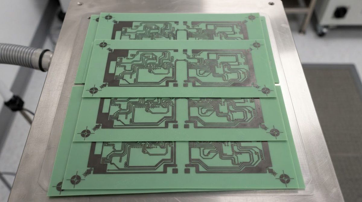
The HTCC process sinters alumina (typically Al₂O₃ 92–96%) green tape in a hydrogen or hydrogen/nitrogen atmosphere at 1,400–1,600 °C. At those temperatures, copper is molten and would diffuse uncontrollably into the ceramic, destroying both the conductor pattern and the substrate’s dielectric properties. Only metals with melting points well above the sintering temperature survive the firing intact.
Tungsten (melting point 3,422 °C) and molybdenum (melting point 2,623 °C) are the standard choices. Both are formulated into screen-printable pastes with ceramic binders that burn out during the firing ramp, leaving a dense metal trace bonded to the ceramic at the molecular level. This co-fired bond is far stronger than any post-applied metallization, which is a primary reason HTCC remains the process of choice for hermetic, multilayer packages in aerospace and military electronics.
HTCC Co-fired Conductor Thickness and Line Capabilities
Conductor geometry in HTCC is set by the screen-printing process applied to unfired green tape. Because the tape and paste shrink together during sintering (typically 15–20% linearly), the as-printed dimensions are larger than the final fired dimensions. All values below are post-shrinkage, fired dimensions.
| Parameter | Typical Range | Unit | Notes |
|---|---|---|---|
| Conductor material | W or Mo | — | W is more common; Mo used where slightly lower resistivity is needed |
| Fired conductor thickness (single pass) | 8–15 | µm | Depends on mesh count, paste viscosity |
| Fired conductor thickness (double print) | 20–30 | µm | Two sequential print-dry cycles before firing |
| Maximum practical thickness | 40–50 | µm | Beyond this, paste cracking and delamination risk increases |
| Minimum fired line width | 75–100 | µm | Finer lines possible with advanced screens, but yield drops |
| Minimum fired line spacing | 75–100 | µm | Limited by paste spread and shrinkage tolerance |
| Sheet resistance (W, 12 µm fired) | 8–12 | mΩ/sq | Per Kyocera and CoorsTek HTCC datasheets |
| Via diameter (fired) | 100–200 | µm | Punched or laser-drilled in green tape before fill |
| Number of co-fired layers | 2–60+ | layers | Military HTCC packages routinely exceed 20 layers |
Typical values for commercially available HTCC processes, for comparison only. Confirm against the datasheet for your specific grade and supplier.
For detailed dimensional constraints and pattern rules, see the HTCC design rules reference.
Resistivity Trade-off: Tungsten vs. Copper
The biggest engineering penalty of HTCC co-fired conductors is resistivity. A worked example makes the impact concrete.
Worked Example: DC Resistance of a 10 mm Trace
Assume a 10 mm long trace, 200 µm wide, 15 µm thick.
Tungsten (ρ = 5.6 µΩ·cm):
R = ρ × L / A = 5.6 × 10⁻⁶ Ω·cm × 1.0 cm / (0.020 cm × 0.0015 cm) = 1.87 Ω
Copper (ρ = 1.7 µΩ·cm):
R = 1.7 × 10⁻⁶ × 1.0 / (0.020 × 0.0015) = 0.57 Ω
The tungsten trace has 3.3× the resistance of the same geometry in copper. For signal interconnects and low-current control lines, this is acceptable. For power buses carrying several amps, it means significant I²R heating and voltage drop. In power-delivery applications, designers either widen traces substantially or move to a different substrate technology.
Post-fire Plating: Making HTCC Solderable
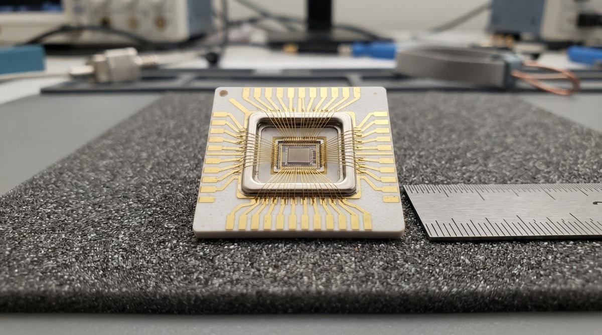
Tungsten and molybdenum oxidize readily and are not directly solderable with standard Sn-Ag-Cu or Sn-Pb alloys. After firing, HTCC substrates receive a nickel barrier layer (typically 2–5 µm electroless Ni) followed by a gold flash (0.5–1.5 µm Au) or thicker gold for wire bonding (1.0–3.0 µm Au). This Ni/Au finish provides solderability, wire-bond compatibility, and corrosion protection. The plating step is a post-fire operation—it does not affect the co-fired conductor’s bulk properties.
For specifics on plating thickness tolerances and adhesion requirements, the ceramic metallization overview covers both co-fired and post-fire options in detail.
HTCC vs. LTCC: Conductor Comparison
| Parameter | HTCC | LTCC | Source / Standard |
|---|---|---|---|
| Firing temperature | 1,400–1,600 °C | 850–900 °C | General industry practice |
| Co-fired conductor metals | W, Mo | Ag, Au, AgPd, Cu (in N₂) | Kyocera, CoorsTek datasheets |
| Conductor resistivity | 5.3–5.6 µΩ·cm (W) | 1.6–1.7 µΩ·cm (Ag) | Bulk values at 20 °C |
| Fired line/space | 75–100 / 75–100 µm | 50–75 / 50–75 µm | Process-dependent |
| Substrate strength (MOR) | 300–400 MPa (96% Al₂O₃) | 200–320 MPa | ASTM C1161, manufacturer data |
| Hermeticity | Excellent—dense alumina | Good—glass-ceramic matrix | MIL-STD-883, method 1014 |
| Dielectric constant (1 MHz) | 9.0–9.8 | 5.0–9.0 (varies by tape) | Manufacturer datasheets |
Typical values for comparison only. Confirm against the datasheet for your specific grade.
LTCC fires below copper’s melting point, so silver and even copper (in controlled nitrogen atmosphere) can be co-fired directly. If low conductor resistance is a priority and the substrate’s mechanical and thermal demands can be met by glass-ceramic, LTCC is usually the better path.
When NOT to Use HTCC
High-current power delivery. If your design requires traces carrying more than a few hundred milliamps with tight voltage-drop budgets, the resistivity of tungsten becomes a real problem. Consider LTCC with silver conductors, or a DBC/AMB substrate with thick copper bonded to a fired alumina or AlN base.
Cost-sensitive, high-volume consumer products. HTCC is expensive per unit. The multi-step green-tape process, hydrogen-atmosphere sintering, and Ni/Au plating add cost that FR-4 or standard aluminium-core MCPCBs avoid entirely.
RF circuits needing low conductor loss. At microwave frequencies, the higher resistivity of tungsten increases ohmic loss in transmission lines. LTCC with silver or gold conductors, or thin-film metallization on fired alumina, offers lower insertion loss. See the thin-film layout guidelines for an alternative approach.
Large substrate sizes. Shrinkage tolerance in HTCC compounds with area. Substrates larger than roughly 100 × 100 mm become difficult to hold to tight positional tolerances.
FAQ
Can you co-fire copper inside an HTCC substrate?
No. Copper melts at 1,085 °C and HTCC fires at 1,400–1,600 °C. The only co-fired conductors compatible with HTCC are refractory metals—tungsten and molybdenum. Copper can be plated or brazed onto the surface after firing, but it is not part of the co-fired structure.
What is the maximum number of layers in an HTCC package?
Production HTCC packages with 40–60+ co-fired layers exist, primarily in military and aerospace hermetic packaging. Layer count is limited mainly by alignment tolerance accumulation and total package height, not by the process itself.
Is HTCC the same as thick-film ceramic?
No. Thick-film metallization is applied to an already-fired (sintered) ceramic substrate. HTCC co-fires the metal and ceramic together from the green state. The bond mechanism, conductor materials, and design rules differ significantly between the two processes.
How does HTCC conductor adhesion compare to post-fire metallization?
Co-fired conductors in HTCC achieve peel strengths of roughly 20–40 N/cm because the metal and ceramic sinter together, forming a mechanical and chemical bond. Post-fire thick-film conductors on alumina typically achieve 10–25 N/cm, depending on the paste system and firing profile. The co-fired bond is inherently more reliable under thermal cycling.
Does HTCC shrinkage affect via registration?
Yes. Linear shrinkage of 15–20% means that a 200 µm via punched in green tape ends up at roughly 160–170 µm after firing. Positional accuracy depends on shrinkage uniformity across the panel. Tight via-to-pad registration requires matched shrinkage control, which is covered in the HTCC layout guidelines.