HTCC (high-temperature co-fired ceramic) substrates are sintered at 1 500–1 600 °C, which means your green-tape layout must account for 15–20 % linear shrinkage, refractory metallization limits, and via aspect-ratio constraints that do not exist in organic PCB design. Following proven HTCC co-fired ceramic layout guidelines prevents warped panels, open vias, and delaminated layers—failures that are expensive because every layer is committed before firing. The guidelines below give you the numbers you need to avoid those outcomes.
What Is HTCC and How Does It Differ from LTCC?
HTCC is a multilayer ceramic process in which alumina (Al₂O₃ 90–96 %) or aluminum nitride green tapes are punched, printed with refractory-metal paste (tungsten or moly-manganese), stacked, laminated, and co-fired in a single high-temperature cycle. The firing temperature—typically 1 500–1 600 °C in a reducing atmosphere—is the defining difference from LTCC layout methods, which fire at 850–900 °C and permit silver or gold conductors.
Because only refractory metals survive the HTCC firing profile, conductor resistivity is higher (W bulk ≈ 5.3 µΩ·cm vs. Ag ≈ 1.6 µΩ·cm). This constrains trace width, current capacity, and RF loss. It also means post-fire plating—usually nickel/gold—is almost always required for solderability.
Shrinkage Compensation: The Biggest Risk in HTCC Co-Fired Ceramic Layout Guidelines
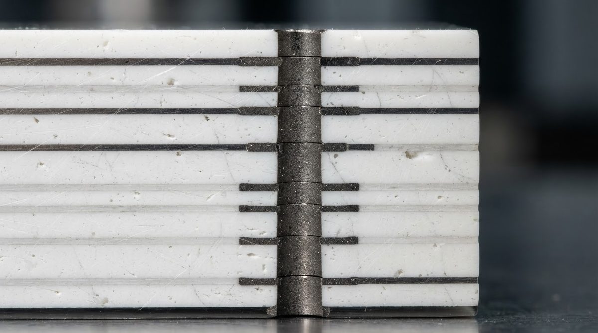
Green alumina tape shrinks 15–20 % linearly during sintering (per CoorsTek and Kyocera published datasheets for 92–96 % Al₂O₃ tape). Shrinkage is repeatable to ±0.3–0.5 % within a lot, but varies between lots and between X and Y directions if the tape has a preferred grain orientation from casting.
Design your artwork at 1/(1 − S) scale, where S is the nominal linear shrinkage fraction supplied by your tape vendor. For 17 % shrinkage, the scale factor is 1.205×. Apply this uniformly to all features: pads, traces, vias, and panel outlines.
Worked Example — Pad Pitch After Shrinkage
Target fired pitch: 0.500 mm. Tape shrinkage: 17 ± 0.4 %. Green-state pitch = 0.500 / (1 − 0.17) = 0.602 mm. Worst-case fired pitch range: 0.500 mm ± (0.602 × 0.004) = 0.500 ± 0.0024 mm. If your component pad tolerance is ±0.025 mm, you have margin. If it is ±0.002 mm (bare-die bonding), you do not—consider post-fire laser trimming or tighter lot control.
Conductor Rules for Refractory Metallization
Tungsten and moly-manganese pastes are screen-printed onto green tape before stacking. Typical print-and-fire capabilities for HTCC co-fired ceramic layout guidelines are narrower than thick-film-on-fired-substrate processes because the paste must survive lamination pressure and high-temperature shrinkage.
| Parameter | Typical HTCC Range | Unit | Condition | Source |
|---|---|---|---|---|
| Min line width | 75–125 | µm | After firing, W paste | Kyocera HTCC design guide |
| Min line space | 75–125 | µm | After firing | Kyocera HTCC design guide |
| Conductor thickness (fired) | 8–15 | µm | Single print | CoorsTek technical bulletin |
| Sheet resistance (W) | 8–12 | mΩ/□ | Fired, 10 µm thick | Kyocera / Maruwa datasheets |
| Pad-to-edge clearance | ≥ 250 | µm | Fired dimension | Industry practice |
Typical values for commercially available material, for comparison only. Confirm against the datasheet for your specific grade.
If your design needs finer traces (below 50 µm) or lower resistivity, consider a hybrid approach: HTCC for the multilayer hermetic body, with thin-film post-fire metallization on the top surface for precision RF or high-density interconnect.
Via Design and Aspect-Ratio Limits
HTCC vias are punched or laser-drilled in green tape, then filled with the same refractory paste. During lamination and firing, the paste must densify without leaving voids. Adhering to these HTCC co-fired ceramic layout guidelines for vias is critical:
- Minimum via diameter (fired): 100–150 µm for mechanical punch; 50–75 µm for laser drill.
- Maximum aspect ratio (depth : diameter): 1:1 to 1.5:1. Beyond this, paste fill becomes unreliable and void rates climb.
- Via-to-via pitch: ≥ 2× via diameter to avoid green-tape tearing during punch.
- Via-to-edge clearance: ≥ 300 µm fired to prevent edge cracking.
Stacked vias (vertically aligned through multiple layers) are standard in HTCC, unlike some organic builds. However, each stacked via adds cumulative positional tolerance. Budget ±25–50 µm per layer in your registration stack-up.
Layer Count and Stackup Considerations
Commercial HTCC packages routinely reach 20–60+ layers (Kyocera and NTK published examples). Each green-tape layer is typically 100–250 µm thick before firing, shrinking to 80–200 µm fired. Total substrate thickness after firing commonly falls between 0.5 mm and 5 mm.
More layers mean longer lamination and higher risk of delamination. Keep ground and power planes on inner layers; route signals on layers closest to the surface where registration is best controlled. Assign at least one continuous ground plane for every four signal layers to manage impedance and crosstalk.
Thermal Via Arrays for Heat Spreading
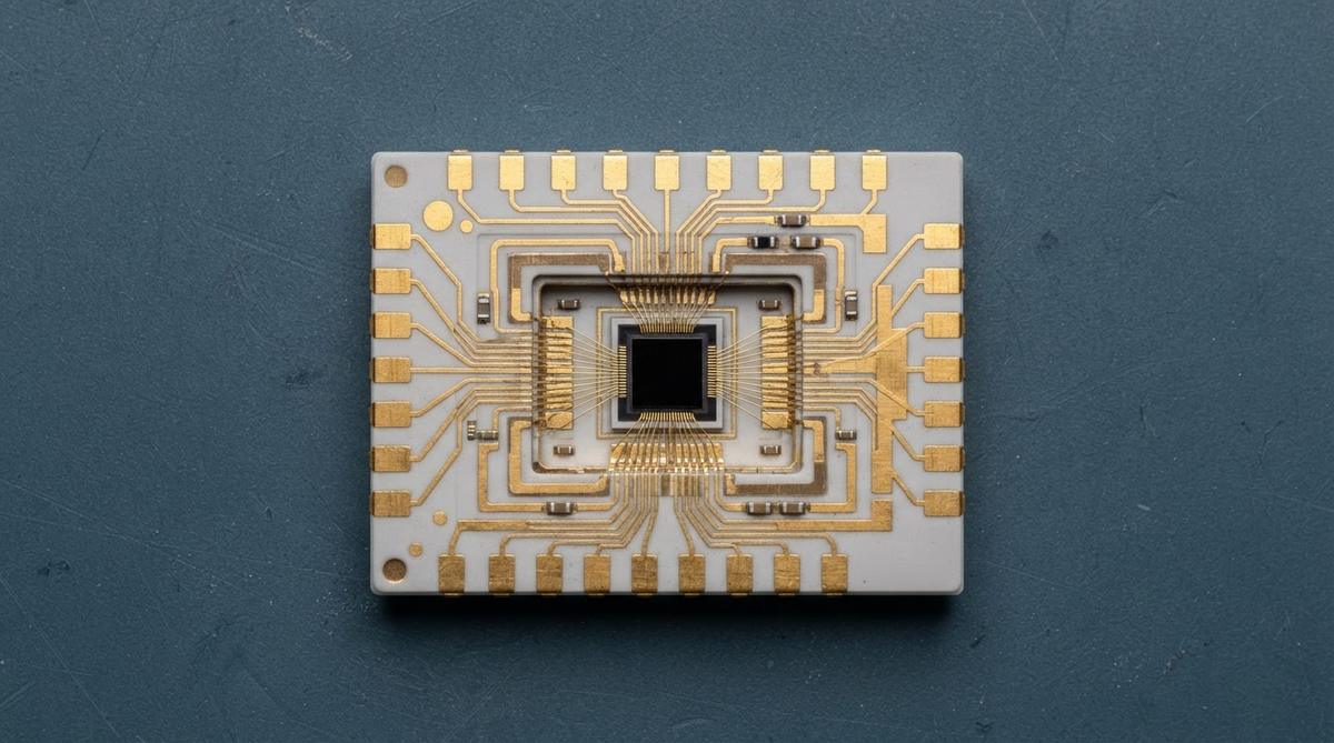
HTCC alumina (96 %) conducts heat at 24–28 W/m·K (per ASTM E1461, manufacturer data). Where a die dissipates significant power, thermal via arrays filled with tungsten (thermal conductivity ≈ 170 W/m·K) can reduce the through-substrate thermal resistance substantially. A 3 × 3 array of 200 µm vias on 500 µm pitch under a 2 mm × 2 mm die can cut Rth by 30–40 % compared to bare ceramic, depending on substrate thickness. Size the array to cover the die footprint and route it to a brazed metal base or heat-sink pad on the bottom layer.
Enter your substrate area, thickness, and thermal via count to estimate the effective through-substrate thermal resistance for your HTCC layout.
Post-Fire Finishing and Plating
Tungsten is not directly solderable. Standard practice is electroless nickel (3–8 µm) followed by electrolytic or immersion gold (0.5–2.5 µm) over all exposed pads. Design your pad geometry to accommodate the plating thickness—add 2× plating buildup to each pad edge when checking clearance to adjacent features. For wire-bond pads, gold thickness of ≥ 1.25 µm is typical to ensure reliable ball or wedge bonding per MIL-STD-883 Method 2011.
If your application also requires brazed seal rings or kovar leads, define those features in the layout with clearance to the nearest conductor of at least 500 µm to prevent solder or braze wicking.
When HTCC Is Not the Right Choice
HTCC excels at hermetic, high-layer-count, high-reliability packages for military, aerospace, and sensor applications. It is not the best fit when:
- Low conductor resistance matters most. Tungsten’s sheet resistance (8–12 mΩ/□) is 5–8× higher than thick-film silver or copper. For power distribution or low-loss RF below 10 GHz, LTCC with silver or a thick-film-on-fired-alumina approach may outperform.
- Budget is tight and hermeticity is not required. HTCC tooling and processing costs are high. Standard alumina with post-fired thick-film metallization covers many sensor and LED applications at lower cost.
- You need rapid prototyping. Green-tape lot procurement, screen sets, and firing profiles make HTCC lead times long—often 8–16 weeks. Thin-film on pre-fired substrates can prototype in days.
Frequently Asked Questions
What materials work as HTCC substrates?
Alumina (Al₂O₃ 90–96 %) is the most common HTCC body material. Aluminum nitride (AlN) is used where higher thermal conductivity is needed (170–200 W/m·K), though it requires nitrogen-atmosphere sintering and costs significantly more. Silicon nitride and zirconia are not processed via HTCC co-firing.
Can I use copper conductors in HTCC?
No. Copper melts at 1 085 °C, well below the 1 500–1 600 °C HTCC sintering range. Only refractory metals—tungsten and molybdenum-manganese—survive the firing cycle. If you need copper conductors in a co-fired ceramic, use LTCC, which fires at 850–900 °C.
How many layers can an HTCC substrate support?
Production HTCC packages commonly reach 20–60 layers, with specialty military and space packages exceeding 100 layers. Layer count is limited mainly by registration tolerance accumulation and total lamination pressure rather than by any fundamental material constraint.
What is the typical positional tolerance after firing?
Feature-to-feature positional accuracy after HTCC sintering is typically ±25–50 µm per layer, with overall panel accuracy of ±0.1–0.3 % of the fired dimension. Tighter tolerances require post-fire laser trimming or mechanical grinding.
Is HTCC hermetic?
Yes. Fully densified HTCC alumina achieves helium leak rates below 1 × 10⁻⁸ atm·cc/s per MIL-STD-883 Method 1014, making it suitable for hermetic packaging of MEMS, sensors, and military hybrid circuits.
Next Step
If your design requires HTCC, prepare your layout with the shrinkage factor, via rules, and conductor limits covered in these HTCC co-fired ceramic layout guidelines, then submit your files for a manufacturability review. For projects where LTCC or post-fired thick-film may be a better fit, our engineers can advise during quoting.