HTCC (high-temperature co-fired ceramic) substrates are sintered at 1500–1700 °C, which limits conductor metals to refractory types—tungsten (W) and molybdenum (Mo)—and demands tight shrinkage control across every layer. The HTCC co-fired ceramic design rules below reflect these physical realities and apply to 92–96% Al₂O₃ and AlN HTCC substrates, the two most common base materials. Understanding these rules before layout prevents costly respin cycles caused by shrinkage mismatch, via voids, or excessive conductor resistance.
Key Takeaways
- HTCC green tape shrinks 15–20% in X-Y and 20–30% in Z during sintering; all features must be pre-scaled accordingly.
- Conductor metals are limited to W and Mo (plus Mo-Mn), with sheet resistances of 8–15 mΩ/sq—roughly 5–10× higher than copper.
- Minimum via diameter after sintering is typically 100–150 µm; aspect ratios above 3:1 are difficult to fill reliably.
- Layer counts of 10–60+ are achievable, but each added layer compounds positional tolerance error from lamination and shrinkage.
- Post-fire plating (Ni/Au) is required for solderability because W and Mo do not wet standard Sn-Ag-Cu solders.
Why HTCC Co-Fired Ceramic Design Rules Differ from LTCC and Thick Film
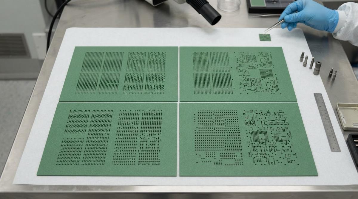
The defining constraint of HTCC is the sintering temperature. At 1600 °C, organic binders burn out of green tape, and alumina or AlN particles densify into a monolithic ceramic body. Only metals with melting points well above 1600 °C survive this process—hence W (mp 3422 °C) and Mo (mp 2623 °C). Copper, silver, and gold melt far below 1600 °C and cannot be used as internal conductors.
This single fact cascades into several design differences compared to LTCC co-fired ceramic design rules, where silver and gold conductors are available because LTCC fires at 850–900 °C. It also means HTCC conductors have higher resistivity, which limits trace density in high-speed digital and RF routing. Every rule in this guide traces back to that temperature constraint.
Shrinkage and Dimensional Tolerances
Green (unfired) HTCC tape shrinks significantly during sintering. Typical X-Y shrinkage is 15–20%, and Z-axis shrinkage is 20–30%, depending on the tape formulation and furnace profile. Manufacturers characterize shrinkage lot-by-lot and pre-scale artwork to compensate, but residual variation remains.
Expect fired dimensional tolerances of ±0.5–1.0% of the nominal dimension for standard production. For a 50 mm substrate, that is ±0.25–0.50 mm. Tighter tolerances—down to ±0.1%—are possible with post-fire lapping and grinding of the ceramic substrate, but this adds cost and is practical only on external surfaces.
Worked Example: Shrinkage Pre-scaling
Suppose the fired target for a via pitch is 1.000 mm and the lot-specific X-Y shrinkage factor is 17.5%. The green-state artwork pitch must be:
Green pitch = 1.000 mm / (1 − 0.175) = 1.000 / 0.825 = 1.212 mm
If shrinkage varies ±0.5% (i.e., 17.0–18.0%), the fired pitch lands between 0.994 and 1.006 mm. When applying HTCC co-fired ceramic design rules to your layout, size pad geometries and annular rings to absorb this range.
Conductor Design Rules for HTCC Co-Fired Ceramic
W and Mo pastes are screen-printed onto green tape before lamination and co-firing. Paste rheology and tape surface roughness set the practical limits.
| Parameter | Typical HTCC Value | Unit | Condition | Source |
|---|---|---|---|---|
| Min. trace width | 75–125 | µm | After sintering; W paste on 96% Al₂O₃ | Kyocera HTCC design guide |
| Min. trace spacing | 75–125 | µm | After sintering | Kyocera HTCC design guide |
| Conductor thickness (per print) | 8–15 | µm (fired) | Single screen pass | CoorsTek technical data |
| Sheet resistance (W) | 8–15 | mΩ/sq | Fired, 10 µm thick | Kyocera HTCC design guide |
| Sheet resistance (Mo) | 7–12 | mΩ/sq | Fired, 10 µm thick | CoorsTek technical data |
| Max. layer count | 10–60+ | layers | Production; higher counts are custom | Industry standard |
Typical values for commercially available material, for comparison only. Confirm against the datasheet for your specific grade.
Because W and Mo resistivity is 5–10× that of copper, power distribution traces must be wider to keep IR drop within budget. For high-current paths, consider thick copper post-fire plating on external surfaces rather than trying to carry current through internal W traces.
Via Design Rules
Vias in HTCC are punched or laser-drilled in green tape, then filled with W or Mo paste before lamination. The green via must be oversized to account for shrinkage, and the fill must remain continuous through sintering. Proper via sizing is one of the most failure-sensitive areas within HTCC co-fired ceramic design rules.
| Parameter | Typical HTCC Value | Unit | Notes |
|---|---|---|---|
| Min. via diameter (fired) | 100–150 | µm | Mechanical punch; laser can reach 75 µm green |
| Max. aspect ratio | 3:1 | — | Higher ratios risk incomplete fill and voids |
| Min. via-to-via pitch | 2× via diameter | — | Center-to-center; accounts for annular ring |
| Min. annular ring | 50–75 | µm | After shrinkage variation |
| Via resistance (100 µm dia, 200 µm deep, W fill) | 15–40 | mΩ | Depends on fill density |
Typical values for commercially available material, for comparison only. Confirm against the datasheet for your specific grade.
Stacked vias are standard in HTCC because each layer is punched and filled independently before lamination. Staggered vias are also used but consume more routing area. For detailed via fill considerations, see via filling for ceramic PCBs.
Substrate and Layer Thickness
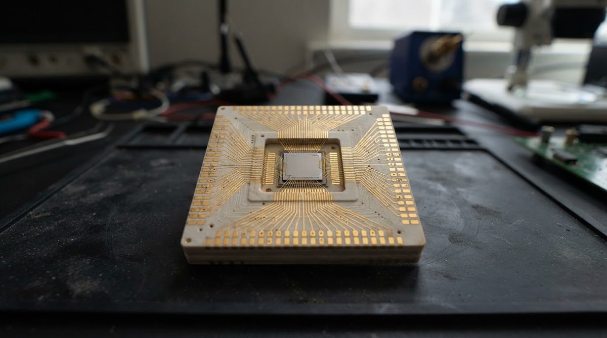
Individual green tape layers are typically 100–300 µm thick (fired). Total substrate thickness for a multilayer HTCC package ranges from 0.5 mm to over 5 mm. Thinner layers improve via aspect ratio but are more fragile during handling. Cavity depths for die attach are controlled by omitting tape layers in the stack.
Post-fire Metallization and Surface Finish
W and Mo surfaces oxidize in air and do not accept solder directly. Standard practice is to plate Ni (3–8 µm) followed by Au (0.5–3.0 µm) over exposed pads after sintering. This Ni/Au finish enables wire bonding and reflow soldering. For more on plating options and tolerances, refer to ceramic metallization capabilities.
Design Rule Checklist
Use this checklist against your layout before submitting files to an HTCC manufacturer. It consolidates the HTCC co-fired ceramic design rules covered above into a pass/fail format:
- All artwork submitted at fired dimensions (manufacturer handles pre-scaling).
- Annular rings ≥ 50 µm after worst-case shrinkage variation.
- Via aspect ratio ≤ 3:1 for all filled vias.
- Power traces widened to compensate for W/Mo sheet resistance (8–15 mΩ/sq).
- Post-fire Ni/Au plating specified on all solder and wire-bond pads.
- Cavity depths defined by integer multiples of fired tape thickness.
Enter your substrate dimensions, layer count, and via geometry below to check whether your design falls within standard HTCC process windows or requires custom tooling.
When Not to Use HTCC
HTCC is the wrong choice when any of the following apply:
- Low conductor resistance is critical. If your design needs sub-milliohm trace resistance or thick copper planes, thick-film or DBC on a pre-fired substrate will outperform HTCC internal conductors.
- Cost is the primary driver. HTCC tooling (tape casting, punch dies, lamination fixtures) and high-temperature furnace time make it more expensive per unit than LTCC or thick film for simple circuits.
- Rapid prototyping is needed. Green tape shrinkage characterization and furnace qualification take time. Thick-film on pre-fired substrates can turn faster for small quantities.
- RF loss must be minimized. W and Mo have higher conductor loss than Ag or Cu. LTCC with silver conductors, or thin-film on polished alumina, will give lower insertion loss at microwave frequencies.
FAQ
What metals can be used inside an HTCC substrate?
Only tungsten (W) and molybdenum (Mo) survive the 1500–1700 °C sintering temperature. Copper, silver, and gold melt well below this range and are used only as post-fire plating on external surfaces.
How many layers can an HTCC substrate have?
Production HTCC packages commonly reach 10–60 layers. Higher counts are feasible but compound positional tolerance errors and increase cost per layer due to lamination complexity.
Can I use HTCC for RF and microwave circuits?
Yes, but with a trade-off. W and Mo conductors have 5–10× the resistivity of silver or copper, so conductor loss is higher. For frequencies above a few GHz where insertion loss matters, LTCC with Ag conductors or thin-film on polished alumina typically performs better.
What causes voids in HTCC vias?
Incomplete paste fill and binder burnout gas are the main causes. Keeping the aspect ratio at or below 3:1, using vacuum-assisted fill, and optimizing the binder burnout ramp rate all reduce void risk.
Do I need to account for shrinkage in my Gerber files?
No. Submit artwork at the final fired dimensions. The HTCC manufacturer pre-scales the artwork to compensate for their lot-specific shrinkage factor. However, you must design pad and annular ring sizes large enough to absorb the ±0.5–1.0% residual shrinkage variation.
Is HTCC hermetic?
Fully densified HTCC alumina and AlN are inherently hermetic. Leak rates below 1 × 10⁻⁸ atm·cc/s (He) are routinely achieved per MIL-STD-883 Method 1014, making HTCC suitable for sealed cavity packages in military and aerospace applications.