Why Silicon Nitride Si3N4 Laser Scribed Substrates Are the Standard
Silicon nitride Si3N4 laser scribed substrates are the preferred singulation method for Si3N4 ceramics because the material’s fracture toughness of 6–7 MPa·√m (per Kyocera SN series datasheets, ASTM C1421) makes it highly resistant to crack propagation but very difficult to cut with a diamond blade without edge chipping. Laser scribing creates a controlled groove—typically 30–70 % of substrate thickness—so the part snaps cleanly along the scribe line with minimal debris and no coolant contamination.
The result is tight dimensional control (±0.05 mm or better on scribe position), smooth break edges, and zero micro-cracks that could become failure initiation sites under thermal cycling. For power-module substrates bonded with Si3N4 AMB active metal brazing copper, crack-free edges are essential to long-term reliability.
How the Silicon Nitride Si3N4 Laser Scribed Process Works
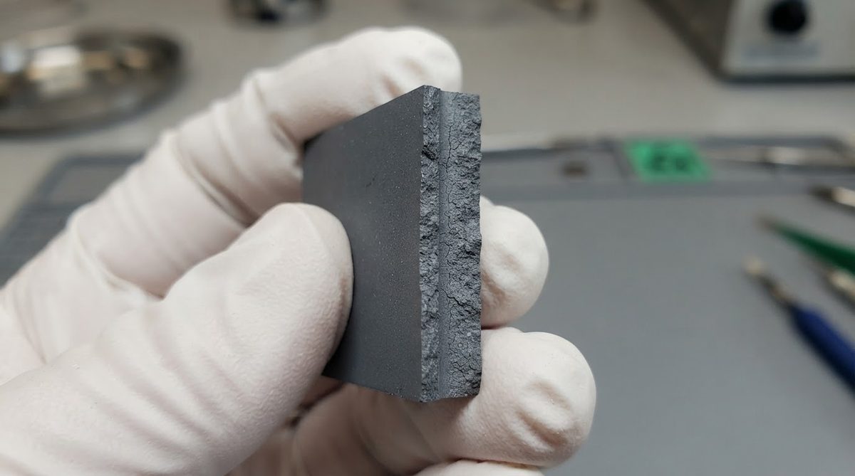
A pulsed laser—usually a CO₂ laser at 10.6 µm or a UV Nd:YAG at 355 nm—traces a groove along the planned break line. The beam ablates material in a narrow kerf (typically 30–80 µm wide) without heating the bulk substrate enough to cause thermal shock. Key process parameters include pulse energy, repetition rate, scan speed, and number of passes.
After scribing, the substrate is broken along the groove either by hand or with a semi-automatic breaker bar. Because Si3N4 is tougher than alumina or aluminum nitride, the scribe depth must be proportionally greater—often 50–70 % of thickness versus 30–40 % for Al₂O₃. Insufficient depth leads to irregular breaks; excessive depth risks through-cuts that damage the copper layer on metallised boards.
The general sequence for producing a silicon nitride Si3N4 laser scribed panel is:
- Fix the substrate or panel to a vacuum chuck on a CNC XY stage.
- Align the laser to fiducial marks or panel edges using a vision system.
- Run the laser along each scribe line at the programmed speed, power, and number of passes.
- Inspect scribe depth with an optical profilometer (target: 50–70 % of substrate thickness).
- Transfer the scribed panel to a breaker station and snap along each groove.
- Inspect break edges under magnification for chipping (< 50 µm acceptable).
Typical Laser Scribing Parameters for Si3N4
| Parameter | Typical Range | Unit | Notes |
|---|---|---|---|
| Laser type | CO₂ or UV Nd:YAG | — | UV preferred for finer kerf |
| Wavelength | 355 / 10,600 | nm | Material absorption varies |
| Kerf width | 30–80 | µm | Depends on beam focus |
| Scribe depth (% of thickness) | 50–70 | % | Higher than Al₂O₃ due to toughness |
| Position accuracy | ±0.03–0.05 | mm | CNC stage dependent |
| Edge chipping after break | < 50 | µm | Typical for optimised process |
| Substrate thickness range | 0.20–1.00 | mm | Thicker substrates need more passes |
Typical values for commercially available Si3N4 substrates, for comparison only. Confirm against the datasheet for your specific grade.
Design Rules for Silicon Nitride Si3N4 Laser Scribed Boards
Place copper traces and pads at least 0.3 mm from the scribe line. Closer spacing risks copper delamination during the break step, especially on Si3N4 DBC substrates where the copper-ceramic bond is under residual stress from the bonding process.
Avoid routing scribe lines through vias or metallised holes. If the layout forces a scribe near a via, increase the keep-out to 0.5 mm minimum. For panelised production, add 0.5–1.0 mm rails between individual units to give the laser room and to provide a clean break zone.
Corner radii matter. Sharp 90° inside corners on scribe patterns concentrate stress and cause irregular breaks. Use a minimum 0.2 mm internal radius at any direction change. For complex outlines that cannot follow straight scribe lines, consider full laser cutting (through-cut) instead of scribe-and-break, accepting a slower cycle time.
Key design keep-outs to remember for silicon nitride Si3N4 laser scribed layouts:
- Copper trace to scribe line: ≥ 0.3 mm
- Via to scribe line: ≥ 0.5 mm
- Panel rail width between units: 0.5–1.0 mm
- Minimum internal corner radius on scribe path: 0.2 mm
- Maximum recommended substrate thickness for scribe-and-break: 1.0 mm
Enter your substrate dimensions and scribe layout to check whether your design stays within safe thermal and mechanical limits.
Laser Scribing vs. Other Singulation Methods
| Method | Edge Quality | Speed | Si3N4 Suitability | Typical Use |
|---|---|---|---|---|
| Laser scribe + break | Clean, < 50 µm chipping | Fast | Excellent | Straight-line singulation |
| Full laser cut | Very clean | Slow (3–5× scribe time) | Good for complex shapes | Non-linear outlines |
| Diamond blade dicing | Risk of chipping > 100 µm | Moderate | Poor—blade wear is high | Al₂O₃, AlN preferred |
| Waterjet | Rough, ±0.1 mm | Moderate | Acceptable for rough blanks | Thick substrates > 1 mm |
Comparison based on industry practice for 0.32 mm Si3N4 substrates.
For related laser processes on ceramic, see laser drilling for ceramic PCBs, which covers via formation rather than singulation.
Material Properties That Affect Scribing
Si3N4’s combination of high fracture toughness (6–7 MPa·√m), moderate thermal conductivity (28–90 W/mK depending on grade, per CoorsTek and Kyocera datasheets at 25 °C), and low coefficient of thermal expansion (2.5–3.2 ppm/°C) makes it behave differently under a laser than alumina or AlN. The high toughness means the scribe groove must be deeper to initiate a controlled fracture. The low CTE means less residual thermal stress around the scribe, which actually improves break-edge quality.
For a deeper look at how thermal conductivity varies by Si3N4 grade and affects substrate selection, see the Si3N4 thermal conductivity guide. If you need polished surfaces before or after scribing, consult the Si3N4 polished substrate page.
When Not to Use Laser Scribing on Si3N4
Laser scribing is the wrong choice in several specific situations. If your substrate is thicker than 1.0 mm and you need complex, non-linear outlines, a full laser cut or waterjet is more reliable—scribe-and-break works best on straight lines. If your production volume is very high (tens of thousands of identical rectangles) and edge-quality requirements are relaxed, diamond dicing of alumina or AlN substrates will be faster and cheaper per unit. Si3N4 itself may be unnecessary if your application does not demand its mechanical toughness or thermal-cycling endurance; comparing ceramic PCB materials can help you decide whether a lower-cost substrate is adequate.
Also, laser scribing leaves a heat-affected zone (HAZ) of 10–30 µm. In applications where the break edge will be a functional surface—such as an optical alignment face—post-scribe grinding or polishing may be needed, adding cost and lead time.
Frequently Asked Questions
Can laser scribing damage copper traces on a metallised Si3N4 board?
Yes, if the scribe line passes too close to copper. Maintaining a 0.3 mm minimum keep-out from the scribe to the nearest trace prevents copper ablation or delamination. Scribing is normally done from the bare ceramic side when both sides are metallised.
What is the thinnest Si3N4 substrate that can be laser-scribed?
Substrates as thin as 0.20 mm are routinely laser-scribed. Thinner material (0.10–0.15 mm) can also be scribed but requires careful fixturing to prevent flexing, which shifts the focal plane and produces uneven grooves.
Does laser scribing weaken the substrate’s mechanical strength?
The scribe groove is a deliberate stress concentrator, so the substrate is weaker along that line by design. Away from the scribe, bulk flexural strength (600–800 MPa per ASTM C1161 for commercial Si3N4 grades) is unaffected because the HAZ is only 10–30 µm deep.
How does silicon nitride Si3N4 laser scribed quality compare to alumina?
Si3N4 laser scribed edges are typically cleaner than alumina edges because Si3N4’s higher toughness resists micro-crack branching. Alumina, being more brittle, can develop lateral cracks that cause chipping beyond the scribe zone. The trade-off is that Si3N4 requires a deeper scribe groove and more laser passes.
Is laser scribing available on panelised Si3N4 production runs?
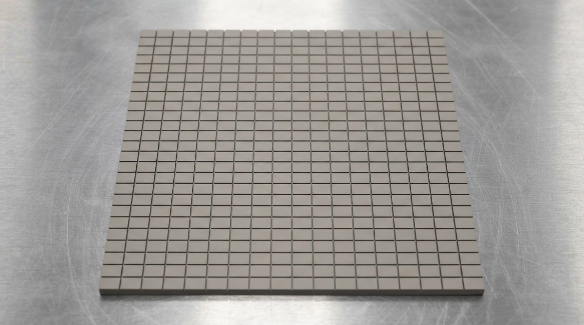
Yes. Panelised scribing is standard for volume production. Panels are scribed in a grid pattern, then broken into individual units. This is the most cost-effective approach for rectangular parts in quantities above a few hundred.
Next Step
If you are specifying silicon nitride Si3N4 laser scribed substrates, prepare a drawing that shows scribe lines, copper keep-outs, and required dimensional tolerances. Upload it for a quote at the Si3N4 substrate ordering page to get pricing based on your exact panel layout and volume.