The ceramic PCB dielectric constant (Dk) for 96% alumina is 9.4–9.8 at 1 MHz, while aluminum nitride sits at 8.6–8.9 and silicon nitride at 7.5–8.5 under the same conditions. These values are three to four times higher than FR-4 (about 4.2–4.5), which means ceramic substrates behave differently in impedance-controlled and high-voltage designs. Understanding the specific dielectric properties of each ceramic grade lets you predict signal behavior, calculate trace geometries correctly, and avoid over- or under-specifying your substrate.
Key Takeaways
- 96% Al₂O₃ has a Dk of 9.4–9.8 at 1 MHz; 99.6% Al₂O₃ rises to 9.7–10.0 (per CoorsTek ADS-996 datasheet).
- AlN offers a slightly lower Dk (8.6–8.9 at 1 MHz) and a dissipation factor under 0.001, making it favorable for high-frequency power circuits.
- Ceramic substrates withstand 10–20 kV/mm dielectric breakdown, roughly ten times higher than standard FR-4 laminate.
- Higher purity alumina raises Dk slightly but lowers the dissipation factor, a trade-off that matters above 1 GHz.
- Si₃N₄ has the lowest Dk among common structural ceramics (7.5–8.5 at 1 MHz), but its primary selection driver is mechanical toughness, not dielectric performance.
What Is Dielectric Constant and Why It Matters for Ceramic PCBs
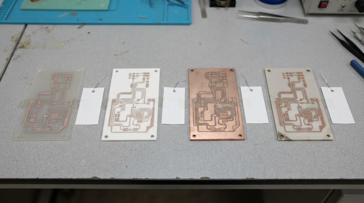
Dielectric constant (Dk, or relative permittivity, εr) describes how much a material concentrates an electric field compared to a vacuum. A higher Dk means more capacitance per unit area between conductors. For PCB traces, that translates to shorter electrical wavelength, tighter coupling between adjacent lines, and narrower trace widths for a given impedance target.
On an alumina substrate with Dk ≈ 9.6, a 50 Ω microstrip trace is roughly half the width it would be on FR-4 (Dk ≈ 4.3) at the same substrate thickness. That can be an advantage when you need compact RF layouts, but it also means tighter manufacturing tolerances on trace width and substrate thickness to hold impedance within spec. Engineers designing for impedance control on ceramic substrates need to account for this from the first stackup iteration.
Dielectric Properties Compared by Material Grade
The table below compiles values from CoorsTek, Kyocera, and Maruwa datasheets for their standard commercial grades. All measurements at 20–25 °C unless noted.
| Material | Dk at 1 MHz | Dk at 10 GHz | Dissipation Factor (tan δ) at 1 MHz | Dielectric Strength (kV/mm) | Volume Resistivity (Ω·cm, 25 °C) | Source |
|---|---|---|---|---|---|---|
| Al₂O₃ 96% | 9.4–9.8 | 9.3–9.7 | 0.0002–0.0010 | 10–15 | >10¹⁴ | CoorsTek ADS-96R |
| Al₂O₃ 99.6% | 9.7–10.0 | 9.6–9.9 | 0.0001–0.0004 | 12–17 | >10¹⁴ | CoorsTek ADS-996 |
| AlN | 8.6–8.9 | 8.5–8.8 | 0.0003–0.0010 | 14–20 | >10¹⁴ | Kyocera SH-30 |
| Si₃N₄ | 7.5–8.5 | 7.4–8.3 | 0.0020–0.0050 | 10–15 | >10¹² | Kyocera SN-220 |
| FR-4 (ref.) | 4.2–4.5 | 4.0–4.3 | 0.015–0.025 | 1.0–1.5 | ~10⁸–10¹⁰ | IPC-4101E, various laminates |
Typical values for commercially available material, for comparison only. Confirm against the datasheet for your specific grade.
A few things stand out. First, the Dk of all ceramic substrates is remarkably stable from 1 MHz to 10 GHz; the shift is typically under 2%. FR-4, by contrast, drops and becomes lossier above a few GHz. Second, dissipation factor for alumina and AlN is one to two orders of magnitude lower than FR-4. Lower tan δ means less signal energy converted to heat, which directly improves insertion loss in RF and mmWave circuits. For a deeper look at how purity affects ceramic substrate performance, including its impact on tan δ, see our dedicated guide.
How Dielectric Constant Affects Trace Width: A Worked Example
Consider a 50 Ω microstrip on a 0.635 mm thick substrate. Using the simplified Hammerstad–Jensen model:
On FR-4 (Dk = 4.3): required trace width ≈ 1.16 mm.
On 96% Al₂O₃ (Dk = 9.6): required trace width ≈ 0.48 mm.
On AlN (Dk = 8.8): required trace width ≈ 0.54 mm.
The ceramic trace is about 40–60% narrower. That is useful for dense RF front-ends, but it also means a ±10 µm etch variation represents a larger percentage of the trace width, so impedance tolerance tightens. If your design calls for ±5% impedance on ceramic, you need trace width control well within ±15 µm, which typically requires thin-film or laser-patterned metallization rather than standard wet-etch thick film.
Dissipation Factor and Its Effect on Signal Loss
Dissipation factor (tan δ) quantifies the fraction of electrical energy lost as heat in the dielectric per cycle. At microwave frequencies, dielectric loss often dominates over conductor loss, especially on smooth ceramic surfaces where skin-effect roughness losses are minimal.
At 10 GHz on a 25 mm long microstrip, the dielectric attenuation contribution on 96% alumina (tan δ ≈ 0.0005) is roughly 0.02 dB. The same trace on FR-4 (tan δ ≈ 0.020) would see about 0.8 dB of dielectric loss. That 40× difference explains why ceramic substrates are standard in radar, satellite, and medical imaging RF chains.
For a full comparison of material properties beyond dielectric behavior, see our overview of Al₂O₃, AlN, Si₃N₄, and BeO ceramic materials.
Dielectric Strength and High-Voltage Isolation
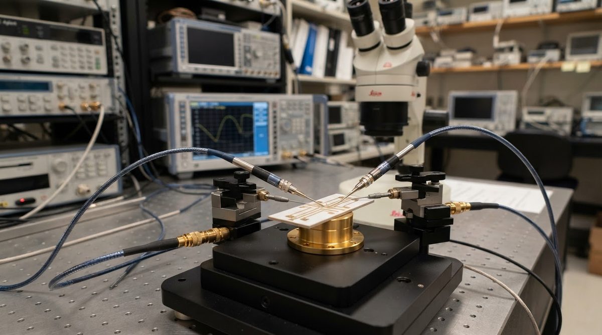
Dielectric strength (breakdown voltage per unit thickness) determines how thin you can make a substrate while still isolating high-voltage circuits. Alumina at 12–15 kV/mm means a 0.635 mm substrate can theoretically withstand over 7.5 kV before breakdown. In practice, designers apply a safety factor of 2–3×, but this still allows ceramic to isolate bus voltages in EV power modules, IGBT drivers, and medical defibrillator circuits without the thick insulation layers organic substrates require.
After fabrication, hipot or dielectric withstand testing verifies that each board meets the required isolation voltage. This is a standard QC step for any ceramic PCB destined for safety-critical applications.
Frequency Dependence: Why Ceramic Dk Stays Flat
Organic laminates contain polar resin molecules that lag behind the applied field at high frequencies, causing Dk to drop and tan δ to rise. Ceramic substrates are crystalline or polycrystalline oxides and nitrides. Their polarization mechanism is ionic and electronic, both of which respond almost instantaneously up to tens of GHz. The result is a Dk that changes less than 2% from DC to 40 GHz for high-purity alumina (per Maruwa HA-96 datasheet), giving designers a stable impedance reference across wide bandwidths.
When Ceramic Dielectric Properties Are Not What You Need
Ceramic is the wrong substrate when low Dk is the primary goal. If you need Dk below 4, materials like Rogers RO4003C (Dk 3.38) or PTFE-based laminates (Dk 2.1–2.5) are better choices and far easier to fabricate in large panels. Ceramic also makes little sense for digital-only boards running below 1 GHz where FR-4 losses are negligible and cost matters most. If your application is purely structural or thermal with no high-voltage or RF requirement, the dielectric properties of the ceramic are irrelevant to your selection; focus on thermal conductivity and CTE instead.
For boards where the ceramic’s mechanical and thermal properties are the real draw, the full range of ceramic substrate types compared can help narrow your choice.
Frequently Asked Questions
Does ceramic PCB dielectric constant change with temperature?
Yes, but the change is small. For 96% alumina, the temperature coefficient of Dk is approximately +100 to +200 ppm/°C between −55 °C and +300 °C (per CoorsTek ADS-96R datasheet). That means a 100 °C temperature swing shifts Dk by about 1–2%, far less than FR-4 over the same range.
Can I get a ceramic substrate with Dk below 7?
Not with standard alumina, AlN, or Si₃N₄. Fused silica (quartz) substrates offer Dk around 3.8 at 1 MHz, and some specialty glass-ceramics reach Dk 5–6. These are niche materials with limited sourcing and higher cost. For most projects needing low Dk, an organic RF laminate is more practical.
Is the dissipation factor of AlN better than alumina?
They are comparable. Both 96% alumina and AlN have tan δ in the 0.0003–0.0010 range at 1 MHz. High-purity 99.6% alumina can beat AlN on tan δ, reaching as low as 0.0001. The primary reason to choose AlN over alumina is thermal conductivity (170–200 W/mK vs. 24–28 W/mK), not dielectric loss.
How does moisture affect ceramic dielectric properties?
Dense, fully sintered ceramics absorb essentially zero moisture (water absorption <0.01% per ASTM C373). Unlike organic laminates, where absorbed water (Dk ≈ 80) can raise effective Dk by 5–10% in humid environments, ceramic Dk remains stable regardless of humidity. This is one reason ceramic substrates are preferred in outdoor radar and satellite systems.
Do metallization layers affect the effective dielectric constant?
The metallization itself does not change the substrate’s Dk, but the metal-ceramic interface and any glass frit in thick-film pastes can create a thin lossy boundary layer. Thin-film metallization (sputtered Ti/Cu or Ti/Pt/Au) avoids glass frit entirely and produces the cleanest dielectric interface, which matters for circuits operating above 10 GHz.
Next Step
If you have a target impedance, operating frequency, and isolation voltage, the next step is matching those to a specific ceramic grade and metallization process. Send your requirements through our instant quote form and our engineering team will recommend a substrate grade and confirm achievable tolerances for your design.
Last reviewed: 2025-07.