An alumina 99.6% Al2O3 thin substrate is a high-purity ceramic sheet—typically 0.1 mm to 1.0 mm thick—used where standard 96% alumina falls short on surface finish, dielectric loss, or thermal performance. The extra 3.6% purity eliminates most of the glassy grain-boundary phase present in 96% grades, raising thermal conductivity from 24–28 W/mK to 30–33 W/mK (at 25 °C) and reducing surface roughness to Ra values below 0.3 µm as-fired, or below 0.025 µm after lapping.
Key Takeaways
- 99.6% alumina thin substrates reach 30–33 W/mK thermal conductivity at 25 °C, roughly 15–20% higher than 96% grades (per Kyocera A-493 and CoorsTek ADS-996 datasheets).
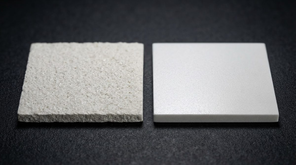
- As-fired surface roughness of Ra ≤ 0.3 µm supports direct thin-film metallisation without mandatory polishing.
- Dielectric constant is 9.7–9.9 at 1 MHz (ASTM D150), with tan δ below 0.0002—critical for low-loss RF and sensor circuits.
- Flexural strength is 400–450 MPa (ASTM C1161, 3-point bend), slightly higher than 96% alumina’s 350–380 MPa range.
- Cost premium over 96% alumina is typically 1.5–2.5× per substrate, depending on size and surface finish requirements.
Why Purity Matters in a Thin Alumina Substrate
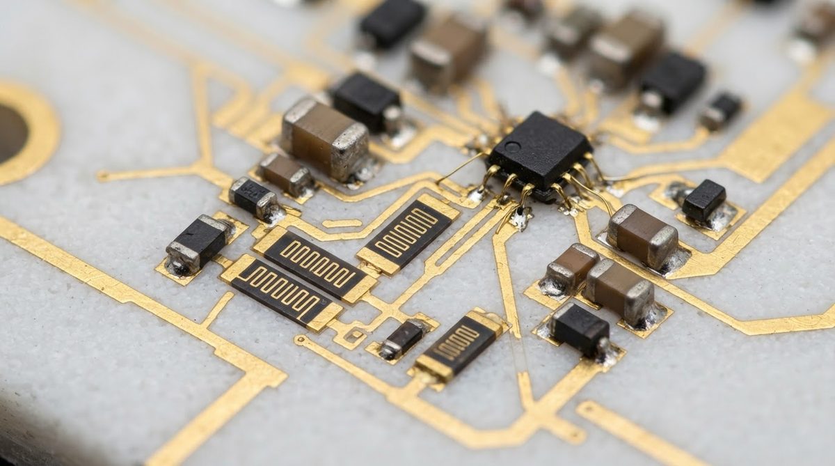
In 96% alumina, the remaining 4% is mostly a silica-based glass phase that bonds grains during sintering. This glass phase is useful—it lowers sintering temperature and cost—but it hurts three things that matter in thin substrates: thermal conductivity, surface finish, and high-frequency dielectric loss.
At 99.6% purity, the glass phase shrinks to a fraction of a percent. Grain boundaries become cleaner, phonon scattering drops, and the substrate surface can be ground or lapped to mirror-like finishes. For thin-film resistor or conductor deposition (sputtered TaN, NiCr, or Au), surface roughness directly controls film uniformity and resistance tolerance. A detailed comparison of how purity affects ceramic substrate performance covers this mechanism in depth.
Material Properties: 99.6% vs 96% Alumina
| Parameter | 99.6% Al2O3 | 96% Al2O3 | Unit | Condition | Source |
|---|---|---|---|---|---|
| Thermal conductivity | 30–33 | 24–28 | W/mK | 25 °C | Kyocera A-493 / CoorsTek ADS-996 |
| Dielectric constant (εr) | 9.7–9.9 | 9.3–9.5 | — | 1 MHz, ASTM D150 | Kyocera / Maruwa |
| Loss tangent (tan δ) | ≤ 0.0002 | 0.0004–0.0011 | — | 1 MHz | Kyocera A-493 |
| Flexural strength | 400–450 | 350–380 | MPa | 25 °C, 3-pt bend, ASTM C1161 | CoorsTek ADS-996 |
| CTE | 7.9–8.1 | 7.4–8.2 | ppm/°C | 25–400 °C | CoorsTek |
| Surface roughness (as-fired) | ≤ 0.3 | 0.5–0.8 | µm Ra | — | Maruwa HA-996 |
| Surface roughness (lapped) | ≤ 0.025 | 0.05–0.10 | µm Ra | — | Maruwa HA-996 |
| Volume resistivity | >10¹⁴ | >10¹⁴ | Ω·cm | 25 °C | Kyocera |
Typical values for commercially available material, for comparison only. Confirm against the datasheet for your specific grade.
The CTE of 99.6% alumina at 7.9–8.1 ppm/°C is a close match to many leadless chip carriers and GaAs die. If your design depends on CTE matching between substrate and die, this grade often avoids the need for a stress-relief interlayer.
Common Thickness Options and Typical Tolerances
Thin substrates in 99.6% alumina are commonly stocked or produced in thicknesses from 0.127 mm (5 mil) to 1.0 mm. Thinner sheets—down to 0.1 mm—are available but require careful handling during metallisation and assembly. Thickness tolerance for as-fired substrates is typically ±0.025 mm; lapped substrates can hold ±0.010 mm or tighter.
For a specific product listing with available sizes and finish options, see the alumina 99.6% thin-film substrate page.
Where 99.6% Alumina Thin Substrates Are Used
Thin-film hybrid circuits. Sputtered or evaporated resistors (TaN, NiCr) and conductors (Au, Cu) need sub-micron surface roughness for tight resistance tolerance. 99.6% alumina is the standard substrate for these circuits in military, aerospace, and medical electronics.
RF and microwave modules. The low tan δ (≤ 0.0002 at 1 MHz, dropping further at higher frequencies relative to 96% grades) reduces insertion loss in stripline and microstrip structures. For more on how ceramic substrates behave at RF frequencies, see dielectric properties of ceramic substrates.
Precision sensor packaging. Pressure sensors, accelerometers, and temperature sensors benefit from the dimensional stability and low outgassing of high-purity alumina.
High-reliability LED and laser submounts. The moderate thermal conductivity (30–33 W/mK) is sufficient for many laser diode submounts where AlN’s cost is not justified.
Worked Example: Thermal Resistance of a 0.25 mm Substrate
A thin-film hybrid dissipates 2 W over a 5 mm × 5 mm footprint on a 0.25 mm thick 99.6% alumina substrate. Estimate the conduction thermal resistance through the substrate.
Rth = t / (k × A)
t = 0.00025 m, k = 31 W/mK (mid-range), A = 0.005 × 0.005 = 2.5 × 10⁻⁵ m²
Rth = 0.00025 / (31 × 2.5 × 10⁻⁵) = 0.32 °C/W
Temperature rise through the substrate alone: ΔT = 2 W × 0.32 °C/W = 0.64 °C. For the same geometry in 96% alumina (k = 26 W/mK), Rth rises to 0.38 °C/W and ΔT to 0.77 °C. The difference is small here, but it scales with power density and becomes meaningful above 10–20 W/cm².
When Not to Use 99.6% Alumina Thin Substrates
Cost-sensitive, high-volume consumer electronics. If your surface finish requirement is Ra > 0.5 µm and your circuit uses thick-film screen printing, 96% alumina does the job at roughly half the substrate cost. The purity premium buys nothing you need.
High-power modules above ~50 W/cm². At extreme power densities, 30–33 W/mK is not enough. Aluminum nitride thin substrates at 170–200 W/mK are the better fit, despite costing 3–5× more.
Mechanically demanding environments. Alumina is brittle. If your substrate faces repeated mechanical shock or vibration with bending loads, silicon nitride (Si3N4) at 600–800 MPa flexural strength and 6–7 MPa·m⁰·⁵ fracture toughness is a more survivable choice.
FR-4 is sufficient. If your operating temperature stays below 130 °C, frequencies are under 1 GHz, and thermal conductivity of 0.3 W/mK is acceptable, there is no reason to pay for ceramic.
Frequently Asked Questions
Can I solder directly to a 99.6% alumina thin substrate?
Not to the bare ceramic. You need a metallisation layer first—typically sputtered Ti/Pt/Au or Ti/Ni/Au for thin-film processes, or screen-printed thick-film conductors. Once metallised, standard reflow or eutectic soldering works normally.
What is the thinnest 99.6% alumina substrate available?
Production substrates are commonly available down to 0.1 mm (100 µm). Below that, handling breakage during metallisation and assembly rises sharply, and most manufacturers recommend 0.127 mm (5 mil) as a practical minimum for circuit use.
Does 99.6% alumina need lapping for thin-film deposition?
It depends on your tolerance requirements. As-fired 99.6% alumina achieves Ra ≤ 0.3 µm, which is adequate for many sputtered conductor layers. For precision thin-film resistors targeting ±0.1% tolerance, lapping to Ra ≤ 0.025 µm is standard practice.
How does 99.6% alumina compare to AlN for laser submounts?
AlN offers 170–200 W/mK thermal conductivity and a CTE of 4.5 ppm/°C, which is a closer match to GaAs and InP die. For high-power laser diodes above ~3 W, AlN is usually necessary. For lower-power lasers and VCSELs, 99.6% alumina at 30–33 W/mK is often sufficient and significantly cheaper.
Is 99.6% alumina compatible with HTCC or LTCC processing?
99.6% alumina substrates are produced by pressing and sintering at 1600–1700 °C, not by the tape-casting and co-firing process used for HTCC or LTCC multilayer circuits. They are single-layer substrates metallised after firing using thin-film or thick-film techniques.
Next Step
If you need volume pricing for 99.6% alumina thin substrates in standard or custom sizes, the 99.6% alumina wholesale page lists available formats. For a quote on a specific design, submit your requirements through the quote request form.