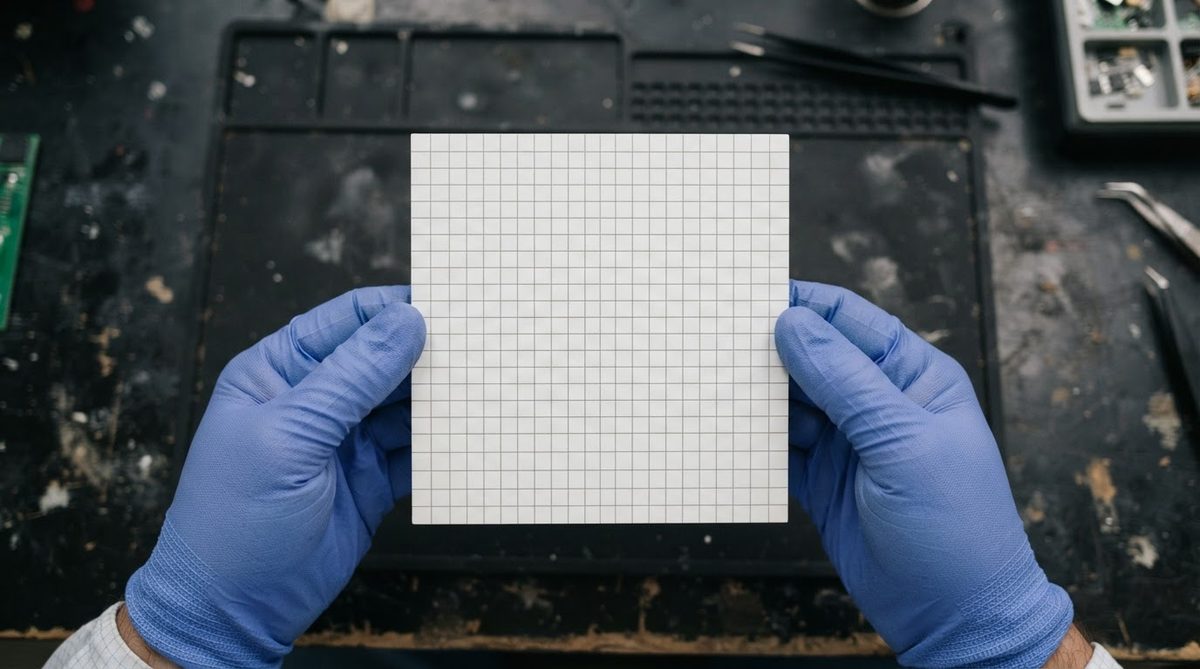
Alumina 96% Al2O3 laser scribed substrates are the most common form of singulated ceramic PCB panels in production today. A focused CO2 or Nd:YAG laser ablates a groove—typically 30–50% of the substrate thickness—along predefined snap lines. After scribing, the panel is broken along those grooves by hand or with a fixture, yielding individual pieces with edge tolerances of ±0.10–0.15 mm. Compared to diamond-wheel scribing, the alumina 96% Al2O3 laser scribed approach produces a narrower kerf, handles tighter radii, and introduces less mechanical stress into the ceramic.
How Laser Scribing Works on Alumina 96% Al2O3 Laser Scribed Panels
The laser beam vaporizes ceramic material along a programmed path, creating a V-shaped or U-shaped groove on one or both sides of the substrate. Groove depth is controlled by laser power, pulse frequency, and traverse speed. A typical single-pass CO2 scribe on 0.635 mm thick 96% alumina produces a groove roughly 0.20–0.25 mm deep with a surface kerf width of 0.05–0.08 mm.
Because the process is non-contact, there is no tool wear and no lateral force on the substrate. This matters for panels that already carry metallization: mechanical scribing can chip copper traces near the snap line, while laser scribing keeps the heat-affected zone (HAZ) to roughly 20–50 µm from the groove edge, per published data from CoorsTek and Kyocera technical notes.
Dual-side scribing is used on substrates thicker than 1.0 mm. Grooves are aligned on opposite faces so the snap propagates cleanly through the full cross-section. Registration between top and bottom grooves must be held within ±0.05 mm to prevent angled fracture surfaces.
Typical Specifications for Alumina 96% Al2O3 Laser Scribed Substrates
| Parameter | Value | Unit | Condition | Source |
|---|---|---|---|---|
| Substrate thickness range | 0.25–2.0 | mm | Standard production | Kyocera A-493 datasheet |
| Scribe groove depth (single side) | 30–50% of thickness | — | CO2 laser, 0.635 mm substrate | Industry practice |
| Kerf width | 0.05–0.10 | mm | CO2 at 10.6 µm wavelength | CoorsTek technical note |
| Snap tolerance (edge to feature) | ±0.10–0.15 | mm | After snap, measured at 20 °C | Industry standard |
| Heat-affected zone | 20–50 | µm | From groove edge | Kyocera / Maruwa data |
| Minimum scribe-to-edge clearance | 0.30 | mm | Recommended for clean snap | Industry practice |
| Thermal conductivity (bulk) | 24–28 | W/mK | At 20 °C, ASTM E1461 | CoorsTek, Kyocera datasheets |
| Flexural strength | 300–380 | MPa | 3-point bend, ASTM C1161 | CoorsTek ADS-96R |
Typical values for commercially available material, for comparison only. Confirm against the datasheet for your specific grade.
For a deeper look at the mechanical properties that determine snap behavior, see alumina 96% flexural strength and reliability data. If your application demands even tighter edge tolerances (below ±0.05 mm), consider specifying a polished or lapped 96% alumina substrate where edges are ground after singulation rather than snapped.
Laser Scribing vs. Diamond-Wheel Scribing
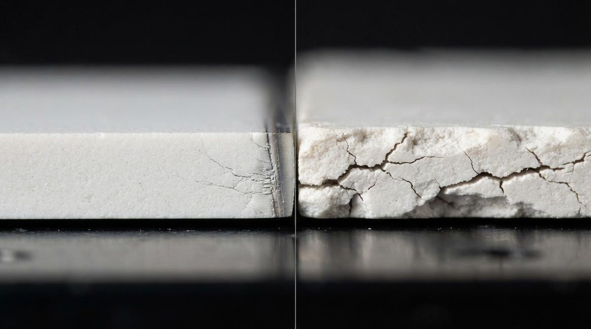
Diamond-wheel scribing uses a rotating blade to score the ceramic surface. It is faster in straight-line throughput but limited in geometry—curves and L-shaped snap paths are not possible. The mechanical contact also generates micro-cracks that propagate 50–100 µm from the groove, roughly double the HAZ of an alumina 96% Al2O3 laser scribed groove.
Laser scribing wins when you need non-linear snap lines, fine pitch between scribe lanes (below 5 mm), or substrates thinner than 0.38 mm where blade pressure risks fracture. Diamond scribing wins on cost for large panels with simple rectangular layouts and substrate thickness above 1.0 mm.
Worked Example: Scribe Lane Width Budget
Suppose you are panelizing 10 × 10 mm substrates on a 101.6 × 101.6 mm (4″ × 4″) panel of 0.635 mm thick 96% alumina. Each scribe lane needs: kerf width (0.08 mm) + snap tolerance on each side (2 × 0.15 mm) + minimum clearance to copper (2 × 0.30 mm) = 0.98 mm total. Rounding to 1.0 mm per lane, you fit 9 columns × 9 rows = 81 units per panel with 1.8 mm of border remaining on each edge for handling.
Design Rules for Alumina 96% Al2O3 Laser Scribed Panels
- Keep copper traces at least 0.30 mm from the snap line. The HAZ and snap deviation together can damage traces closer than this.
- Avoid vias within 0.50 mm of a scribe groove. The stress concentration around a via can redirect the snap path.
- Orient scribe lines parallel to the substrate’s grain direction (if green-tape cast). Snaps perpendicular to grain produce rougher edges.
- Specify groove depth as a percentage of thickness rather than an absolute number. A 40% groove on 0.635 mm stock (0.25 mm deep) snaps cleanly; the same absolute depth on 1.0 mm stock (only 25%) may not.
For substrates where dielectric performance near the edge is critical—such as RF filter housings—request a post-snap edge inspection to verify that micro-cracking has not compromised the surface.
When Laser-Scribed 96% Alumina Is Not the Right Choice
If your substrate must survive operating temperatures above 800 °C or needs thermal conductivity above 100 W/mK, 96% alumina is not the material—consider laser-scribed aluminum nitride (AlN) instead. If you need edge straightness below ±0.05 mm, laser scribing alone will not get you there; you need post-singulation grinding or laser cutting (full through-cut), which costs more. For very high-volume rectangular parts with no metallization, punching from green tape before sintering is cheaper than laser scribing fired substrates. And if your design requires L-shaped cutouts or internal windows, full laser cutting or ultrasonic machining replaces scribing entirely.
Comparing Laser-Scribed Substrates Across Ceramic Materials
| Parameter | 96% Al2O3 | 99.6% Al2O3 | AlN | Si3N4 |
|---|---|---|---|---|
| Thermal conductivity (W/mK) | 24–28 | 28–35 | 170–200 | 70–90 |
| Flexural strength (MPa) | 300–380 | 350–400 | 300–350 | 700–900 |
| Laser scribe ease | Good | Good | Moderate (higher power needed) | Difficult (very tough) |
| Typical snap tolerance (mm) | ±0.10–0.15 | ±0.10–0.15 | ±0.10–0.15 | ±0.15–0.20 |
| Relative substrate cost | 1× | 1.5–2× | 3–5× | 4–6× |
Typical values for commercially available material, for comparison only. Confirm against the datasheet for your specific grade.
Silicon nitride’s high fracture toughness (6–7 MPa·√m vs. 3.5–4 MPa·√m for 96% alumina per ASTM C1421) makes it harder to snap cleanly, so Si3N4 laser scribing often requires deeper grooves or full through-cuts.
Frequently Asked Questions
Can you laser scribe a panel that already has thick-film metallization?
Yes. The laser path is programmed to avoid metallized areas, and the HAZ (20–50 µm) is narrow enough to leave traces 0.30 mm or more from the groove unaffected. Verify with your fabricator that scribe alignment registration is tighter than your trace-to-edge clearance.
Does laser scribing weaken the substrate?
The scribe groove is a deliberate stress concentrator—that is how the snap works. Away from the groove, the bulk flexural strength (300–380 MPa for 96% alumina per ASTM C1161) is unaffected. After snapping, the broken edge is rougher than a ground edge but does not propagate cracks into the body of the part under normal handling.
What is the minimum substrate thickness for laser scribing?
Substrates as thin as 0.25 mm can be laser scribed, though handling becomes the limiting factor. Below 0.38 mm, panels are typically scribed on a vacuum chuck and snapped with a roller fixture rather than by hand.
How does laser scribing cost compare to laser full-cut?
Laser scribing is roughly 30–50% cheaper per panel than full through-cutting because the laser only removes 30–50% of the material thickness. Full cutting is slower, uses more energy, and generates more debris. Choose full cutting only when you need tighter edge tolerances or non-straight geometries.
Is CO2 or Nd:YAG better for scribing 96% alumina?
CO2 lasers (10.6 µm wavelength) are the standard choice. Alumina absorbs strongly at this wavelength, so material removal is efficient. Nd:YAG (1.064 µm) is used when finer kerf widths below 0.05 mm are needed, but at lower throughput and higher equipment cost.