Aluminum nitride (AlN) is the preferred sensor ceramic substrate AlN PCB choice when a device generates concentrated heat or requires a coefficient of thermal expansion (CTE) closely matched to silicon. AlN delivers 170–200 W/mK thermal conductivity at 20 °C (per Kyocera and Maruwa datasheets), a CTE of 4.5–4.7 ppm/°C that sits within 15 % of silicon’s 2.6–3.5 ppm/°C, and volume resistivity above 10¹⁴ Ω·cm. These three properties together make it the substrate of choice for infrared detectors, pressure sensors, gas sensors, accelerometers, and MEMS microphones where thermal drift directly degrades measurement accuracy.
Key Takeaways
- AlN thermal conductivity (170–200 W/mK) is 6–8× higher than 96 % alumina (24–28 W/mK), reducing sensor junction temperature rise.
- A CTE of 4.5–4.7 ppm/°C minimizes die-attach stress when bonding silicon MEMS dies directly to a sensor ceramic substrate AlN PCB.
- Dielectric strength of 15–17 kV/mm (per CoorsTek SN-AlN datasheet, ASTM D149) provides reliable electrical isolation even at sub-millimetre substrate thicknesses.
- AlN substrates cost 3–5× more per unit area than 96 % alumina, so the performance gain must justify the spend.
- For sensors operating below 80 °C with modest power, 99.6 % alumina often delivers adequate performance at lower cost.
Why Sensors and MEMS Need a Sensor Ceramic Substrate AlN PCB
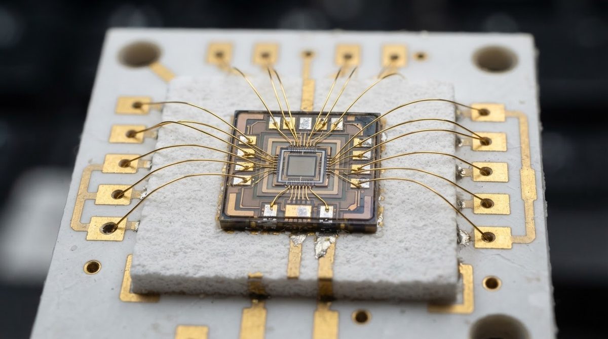
Precision sensors convert a physical quantity—pressure, acceleration, infrared flux—into an electrical signal. Any thermal gradient across the die or package shifts calibration. A substrate that conducts heat away quickly and expands at the same rate as the die keeps the sensor within spec across its operating range.
AlN addresses both problems simultaneously. Its thermal conductivity spreads heat from a concentrated source across the substrate plane, while its CTE prevents cyclic mechanical stress at the die-attach interface during thermal excursions. For a MEMS pressure sensor cycling between −40 °C and +125 °C, the CTE mismatch between die and substrate is the dominant driver of solder-joint fatigue. Switching from 96 % alumina (CTE 6.5–7.0 ppm/°C) to AlN (4.5–4.7 ppm/°C) cuts the mismatch from roughly 4 ppm/°C to about 1.5 ppm/°C, extending solder-joint life by an order of magnitude per Coffin–Manson estimates.
AlN vs. Alumina for Sensor Ceramic Substrate AlN PCB Designs
| Parameter | AlN | Al₂O₃ 96 % | Al₂O₃ 99.6 % | Unit | Condition | Source |
|---|---|---|---|---|---|---|
| Thermal conductivity | 170–200 | 24–28 | 28–35 | W/mK | 20 °C | Kyocera / Maruwa datasheets |
| CTE | 4.5–4.7 | 6.5–7.0 | 6.9–7.2 | ppm/°C | 20–300 °C | CoorsTek |
| Dielectric strength | 15–17 | 10–15 | 12–16 | kV/mm | ASTM D149 | CoorsTek / Kyocera |
| Volume resistivity | >10¹⁴ | >10¹⁴ | >10¹⁴ | Ω·cm | 25 °C | Kyocera |
| Flexural strength | 300–400 | 300–380 | 350–400 | MPa | ASTM C1161 | Maruwa |
| Relative cost (per cm²) | 3–5× | 1× | 1.5–2× | — | — | Market pricing |
Typical values for commercially available material, for comparison only. Confirm against the datasheet for your specific grade.
The table shows that AlN wins on thermal conductivity and CTE match. Alumina wins on cost and availability. If your sensor dissipates less than 0.5 W and operates in a narrow temperature band, a 99.6 % alumina thin substrate may be the smarter economic choice.
Worked Example: Thermal Resistance of a Sensor Ceramic Substrate AlN PCB
Consider an infrared thermopile sensor die (3 mm × 3 mm) dissipating 0.2 W, mounted on a 0.38 mm thick AlN substrate. We estimate the conduction thermal resistance through the substrate directly beneath the die.
Rth = t / (k × A)
Where t = 0.38 mm = 0.00038 m, k = 180 W/mK (mid-range AlN), A = 3 mm × 3 mm = 9 × 10⁻⁶ m².
Rth = 0.00038 / (180 × 9 × 10⁻⁶) = 0.23 °C/W
Temperature rise through the substrate: ΔT = 0.2 W × 0.23 °C/W = 0.047 °C.
Repeating the calculation with 96 % alumina (k = 26 W/mK): Rth = 0.00038 / (26 × 9 × 10⁻⁶) = 1.62 °C/W, giving ΔT = 0.32 °C. For a precision temperature sensor with ±0.1 °C accuracy, that 0.27 °C difference matters. For a motion sensor with ±5 % tolerance, it does not.
Enter your own substrate dimensions and power dissipation below to estimate junction temperature rise for your sensor ceramic substrate AlN PCB design.
Common Sensor and MEMS Applications on AlN
Infrared and Thermal Sensors
Thermopile arrays and bolometers require minimal thermal crosstalk between pixels. AlN’s high in-plane conductivity equalises the heat sink beneath the detector while its low CTE protects fragile MEMS membrane structures during reflow. This same thermal performance makes AlN a strong fit for thermoelectric cooler substrates used to stabilise detector temperatures.
Pressure and Gas Sensors
Silicon MEMS pressure dies bonded with AuSn or SAC305 solder benefit from the tight CTE match. Gas sensors operating at elevated temperatures (up to 300–400 °C for metal-oxide types) stay within AlN’s safe continuous-use range.
RF MEMS and Acoustic Sensors
AlN’s low dielectric loss tangent (tan δ ≈ 0.0003–0.001 at 1 MHz, per Kyocera) makes it suitable for RF MEMS filters and MEMS microphones where parasitic losses degrade signal quality. For designers evaluating different substrate materials for these applications, a comparison of ceramic substrate types provides broader context.
Design Considerations for AlN Sensor PCBs
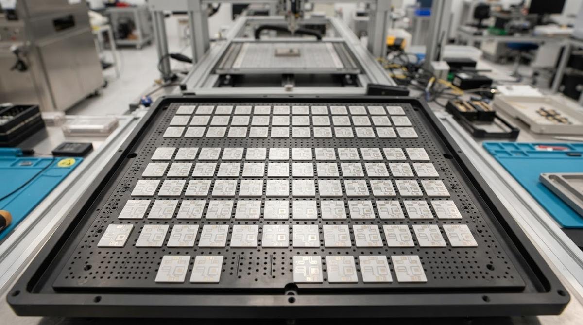
Metallisation. Thin-film sputtered TiW/Au or Ti/Pt/Au is standard for fine-pitch sensor interconnects. Thick-film printing is possible but limited to wider traces. For applications requiring very smooth surfaces for wire bonding, polished AlN substrates with Ra below 0.1 µm are available.
Moisture sensitivity. AlN hydrolyses slowly in humid environments. Exposed surfaces should be protected with a passivation layer (SiO₂, Si₃N₄ thin film) or the assembly should be hermetically sealed. This is especially important for sensors deployed outdoors or in automotive under-hood environments.
Mechanical handling. AlN is a ceramic—it is brittle. Substrate thickness below 0.25 mm requires careful handling fixtures and vacuum pick-and-place. Panel singulation by laser scribing is preferred over mechanical breaking for sensor-grade parts. Thinner substrates are available as AlN thin substrates down to 0.25 mm or less.
Via formation. Laser-drilled or punched vias filled with tungsten paste (co-fired) provide thermal and electrical paths. Minimum via diameters for AlN are typically 0.1–0.15 mm, depending on substrate thickness and process.
When Not to Use AlN for Sensors
AlN is not always the right answer. Choose a different substrate when:
- Power dissipation is below 0.1 W and temperature range is narrow. 96 % or 99.6 % alumina handles this at a fraction of the cost.
- The sensor die is GaAs or another III-V with CTE above 6 ppm/°C. Alumina’s CTE is a closer match.
- Budget is the primary constraint. A sensor ceramic substrate AlN PCB costs 3–5× more per cm² than alumina. For high-volume consumer sensors, that premium may not be recoverable.
- The operating environment is persistently humid without hermetic sealing. AlN’s surface hydrolysis can degrade metallisation adhesion over time.
- Extreme mechanical shock is expected. Silicon nitride (Si₃N₄) offers higher fracture toughness (6–7 MPa·√m vs. AlN’s 2.5–3.5 MPa·√m) for harsh-environment sensors. See how to choose the right ceramic substrate for a broader decision framework.
Frequently Asked Questions
What is the maximum continuous operating temperature of an AlN substrate?
AlN substrates themselves are stable to approximately 1000 °C in inert or nitrogen atmospheres. In air, surface oxidation becomes significant above 700 °C. The practical limit for a metallised sensor ceramic substrate AlN PCB is set by the metallisation and solder, typically 350–450 °C for thick-film systems and around 300 °C for thin-film Au-based systems.
Can I wire-bond directly to an AlN sensor substrate?
Yes. Gold or aluminium wedge bonding works well on AlN with sputtered Ti/Pt/Au or TiW/Au metallisation. Surface roughness should be below Ra 0.4 µm for reliable bonding; polished substrates achieve Ra below 0.1 µm.
Does AlN require special storage conditions?
Bare AlN substrates should be stored in dry, sealed packaging (nitrogen-purged bags with desiccant). Prolonged exposure to humidity above 85 % RH can cause surface hydrolysis, forming aluminium hydroxide that weakens metallisation adhesion.
Is AlN compatible with standard SMT reflow profiles?
AlN withstands lead-free reflow temperatures (peak 260 °C) without any substrate degradation. The concern is not the substrate but the metallisation system and any prior die-attach materials, which must tolerate the reflow profile without re-melting.
How thin can an AlN sensor substrate be?
AlN substrates are commercially available down to 0.15 mm thickness. Below 0.25 mm, handling breakage rates increase and vacuum tooling becomes essential during assembly. Thinner substrates also reduce thermal spreading, so there is a design trade-off between package height and thermal performance.
Next Step
If your sensor or MEMS project requires AlN substrates, start by defining the die size, power dissipation, and operating temperature range. These three parameters determine whether AlN’s cost premium is justified. For volume pricing on AlN sensor substrates, request a wholesale quote with your panel dimensions and annual quantity.