Aluminum nitride (AlN) ceramic is the dominant laser diode submount AlN PCB material for photonics packaging because it solves two problems at once: it conducts heat at 170–200 W/mK (per Kyocera SH-170 and Maruwa HA-200 datasheets) and its coefficient of thermal expansion (CTE) of 4.5–4.7 ppm/°C closely matches GaAs (5.7 ppm/°C) and InP (4.6 ppm/°C). That CTE match keeps solder joints intact over thousands of thermal cycles, which directly determines laser diode lifetime.
Key Takeaways
- AlN thermal conductivity of 170–200 W/mK at 25 °C removes heat 6–8× faster than 96% alumina (24–28 W/mK).
- CTE mismatch between AlN and InP is less than 0.2 ppm/°C, minimizing die-attach stress and wavelength drift.
- Submount thicknesses of 0.25–0.635 mm are standard; thinner substrates reduce thermal resistance but require careful handling.
- Gold (Au) or gold-tin (AuSn) metallization on AlN enables reliable eutectic die attach at 280 °C.
- AlN costs 3–5× more per unit area than 96% alumina, justified only when thermal or CTE requirements demand it.
Why a Laser Diode Submount AlN PCB Outperforms Other Substrates
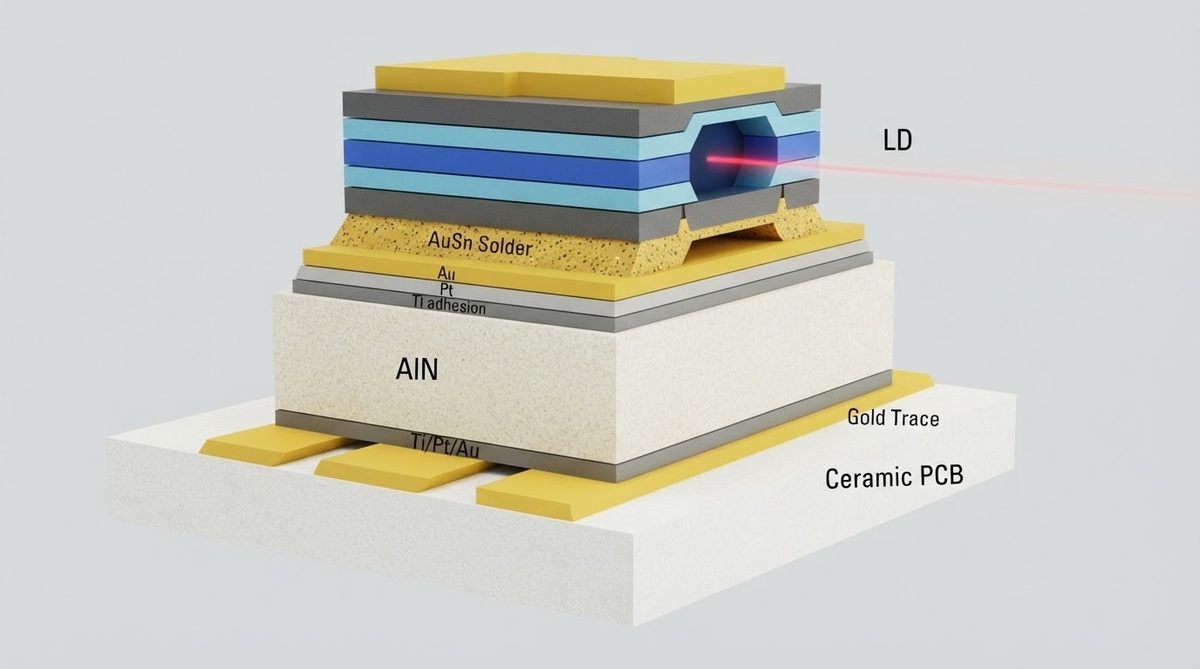
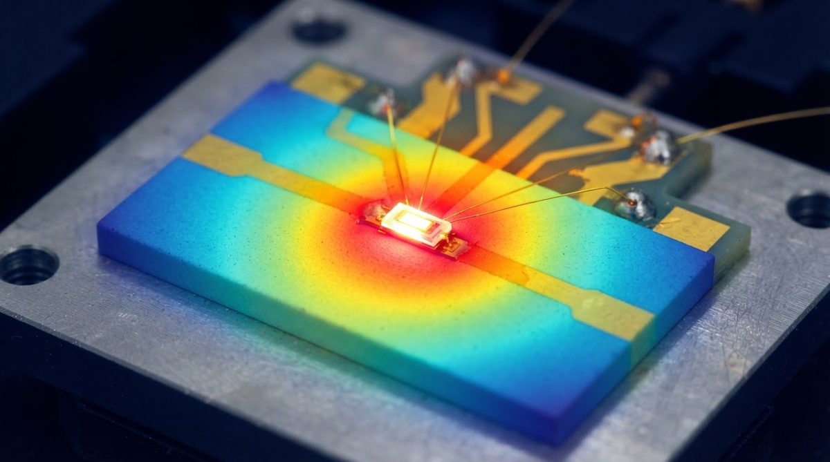
A laser diode converts electrical power to light at roughly 30–60% efficiency. The rest becomes heat, concentrated in an active region a few micrometers wide. A 10 W pump laser dissipating 7 W of waste heat in a 500 µm × 1 mm footprint produces a heat flux above 1,400 W/cm². The submount must spread that heat laterally and conduct it downward to a heatsink before the junction temperature rises enough to shift the emission wavelength or degrade the facet.
FR-4 (0.3 W/mK) and standard metal-core PCBs (1–3 W/mK) are irrelevant at these flux densities. Even 96% alumina laser-scribed substrates fall short in high-power single-emitter and bar applications. The laser diode submount AlN PCB, with thermal conductivity of 170–200 W/mK, is the minimum practical choice for diodes above about 2 W per emitter.
CTE is equally critical. A laser die bonded with AuSn solder at 280 °C cools to 25 °C after assembly. If the submount CTE differs significantly from the die, thermomechanical stress warps the chip, shifts the cavity length, and causes wavelength drift. For telecom DFB lasers operating at 1,550 nm, even 0.1 nm of wavelength shift matters. AlN’s 4.5 ppm/°C CTE keeps stress below the threshold that causes measurable drift in InP-based devices.
Material Properties: AlN vs. Alternatives for Photonics Submounts
| Parameter | AlN | 96% Al₂O₃ | CuW (80/20) | CVD Diamond | Unit | Condition |
|---|---|---|---|---|---|---|
| Thermal conductivity | 170–200 | 24–28 | 180–200 | 1,200–1,800 | W/mK | 25 °C |
| CTE | 4.5–4.7 | 6.5–7.2 | 6.5–8.3 | 1.0–1.5 | ppm/°C | 20–300 °C |
| Dielectric strength | 15–17 | 10–15 | N/A (conductor) | >10 | kV/mm | ASTM D149 |
| Density | 3.26 | 3.72 | 15.6 | 3.52 | g/cm³ | — |
| Relative cost (per cm²) | 1× | 0.2–0.3× | 1.5–3× | 10–30× | — | Indicative |
Typical values for commercially available material, for comparison only. Confirm against the datasheet for your specific grade. AlN values from Kyocera SH-170 and Maruwa HA-200; Al₂O₃ from CoorsTek ADS-96R; CuW from Plansee; CVD diamond from Element Six.
CuW matches AlN on thermal conductivity but is electrically conductive and heavier. It works for non-isolated submounts where weight is acceptable. CVD diamond is thermally superior but its CTE of 1.0–1.5 ppm/°C creates a large mismatch with GaAs, requiring compliant solder layers, and the cost is prohibitive outside military and space programs. For most photonics designs, the laser diode submount AlN PCB strikes the best balance of thermal performance, CTE compatibility, and cost.
Thermal Design: A Worked Example for an AlN Submount
Consider a 5 W single-emitter laser diode at 40% wall-plug efficiency, dissipating 3.33 W of heat. The die footprint is 0.5 mm × 1.0 mm. The submount is 0.38 mm thick AlN (k = 180 W/mK).
One-dimensional thermal resistance through the submount:
Rth = t / (k × A) = 0.00038 / (180 × 0.5 × 10⁻⁶) = 4.2 °C/W
Temperature rise through the submount alone: ΔT = 3.33 W × 4.2 °C/W ≈ 14 °C. In practice, lateral heat spreading reduces this. A finite-element model typically shows 8–11 °C for this geometry. With 96% alumina at 26 W/mK, the same calculation gives Rth = 29.2 °C/W and ΔT ≈ 97 °C—far too high for reliable operation.
This example shows why AlN is not optional for high-power laser submounts. A junction temperature increase of 80+ °C above the heatsink would cut diode lifetime by an order of magnitude, per Arrhenius-based reliability models (see Telcordia GR-468).
Enter your substrate area, thickness, and dissipated power below to estimate junction temperature rise for your own laser diode submount AlN PCB design.
Metallization and Die Attach for Laser Submounts
AlN submounts for laser diodes require metallization that is solderable, wire-bondable, and stable at die-attach temperatures. The standard stack is Ti/Pt/Au or TiW/Ni/Au, deposited by sputtering or e-beam evaporation. Gold thickness is typically 0.5–3.0 µm depending on whether eutectic AuSn solder (80Au/20Sn, melting at 280 °C) or soft indium solder (157 °C) is used.
AuSn eutectic is preferred for telecom and industrial lasers because it is fluxless, provides a void-free bond, and is stable at operating temperatures up to 125 °C. Indium is used for temperature-sensitive devices or when CTE compliance is needed, but it creeps under sustained stress and limits operating temperature.
Surface finish matters. Polished AlN substrates with surface roughness below Ra 0.1 µm improve solder wetting uniformity and reduce voids, directly affecting thermal resistance at the die-submount interface. For thin AlN substrates (0.25 mm or less), handling fixtures during metallization become essential to avoid cracking.
Common Photonics Applications for AlN Submounts
Single-emitter pump lasers (976 nm, 1,480 nm) for fiber amplifiers use AlN submounts almost universally. Telecom DFB and EML lasers on InP use AlN for CTE matching. High-power diode bars and stacks use AlN or AlN-clad CuW for the combination of thermal performance and electrical isolation.
Beyond laser diodes, AlN submounts appear in photodetector packaging, UV and UV-C LED modules, silicon photonics interposers, and thermoelectric cooler assemblies used to stabilize laser wavelength. In each case, the combination of thermal conductivity, electrical isolation, and CTE compatibility drives the choice.
When Not to Use an AlN Submount
A laser diode submount AlN PCB is overkill for low-power VCSELs (< 50 mW) used in data communication. These devices generate minimal heat, and 96% alumina or even ceramic-filled organic substrates handle the thermal load at a fraction of the cost.
If your laser die is GaN-on-SiC (CTE ~4.2–4.7 ppm/°C), AlN remains a good match. But for GaN-on-sapphire (CTE ~7.5 ppm/°C), alumina’s CTE of 6.5–7.2 ppm/°C is actually closer, and the lower cost may justify the thermal trade-off at power levels below 1–2 W.
For purely mechanical carrier applications with no electrical isolation requirement, CuW or CuMo composites offer comparable thermal performance and can be machined to tighter dimensional tolerances than ceramic.
FAQ
What thickness should I specify for a laser diode AlN submount?
Most laser diode submounts use 0.25 mm or 0.38 mm thick AlN. Thinner substrates reduce thermal resistance but are fragile and harder to handle during die attach. Choose 0.25 mm for high-flux single emitters and 0.38 mm for easier processing in lower-power applications.
Can I use AlN submounts with lead-free solder?
Yes, SAC305 (Sn96.5/Ag3.0/Cu0.5, melting at 217–220 °C) works on properly metallized AlN. However, most photonics houses prefer AuSn eutectic for its fluxless process and lower void rates. Lead-free solders generally require flux, which can contaminate optical facets.
How does AlN compare to BeO for laser submounts?
BeO offers 260–300 W/mK thermal conductivity and a CTE of 6.7 ppm/°C. It outperforms AlN thermally but its dust is a confirmed human carcinogen causing chronic beryllium disease. Most photonics manufacturers have eliminated BeO from new designs due to regulatory and handling risks. For detailed safety information, see the beryllia safety guidelines on this site.
Does AlN absorb at common laser wavelengths?
AlN is transparent in the infrared above roughly 1 µm and begins absorbing in the deep UV below 200 nm. For 808 nm, 976 nm, 1,310 nm, and 1,550 nm laser diodes, scattered light hitting the submount surface does not cause measurable absorption or heating.
What dimensional tolerances are achievable on AlN submounts?
Laser-scribed and snapped AlN submounts typically hold ±0.05–0.10 mm on length and width. For tighter tolerances (±0.025 mm), post-firing diamond grinding or laser cutting is required. Discuss your tolerance requirements early—tight tolerances on small parts add significant cost.