A ceramic PCB reflow profile must account for higher thermal conductivity, lower CTE, and greater thermal mass compared to FR-4. Using a standard organic-board profile on a ceramic substrate risks thermal shock cracking, tombstoning from uneven heating, or insufficient wetting from too-short time above liquidus (TAL). The adjustments are straightforward once you understand the three variables that change: ramp rate, TAL, and peak temperature delta across the board.
Key Takeaways
- Limit the heating ramp to 1.5–2.5 °C/s for 96% alumina and 1.0–2.0 °C/s for AlN to avoid thermal shock fracture.
- Time above liquidus (TAL) for SAC305 on ceramic should be 60–120 s, toward the upper end of the J-STD-020E window, because the substrate acts as a heat sink.
- Peak board-surface temperature for SAC305 on ceramic typically needs to reach 245–250 °C to ensure full wetting, versus 235–245 °C on FR-4.
- Cooling rate should stay below 3 °C/s to prevent micro-cracks at solder-to-ceramic interfaces driven by the CTE mismatch between SAC305 (~21 ppm/°C) and alumina (~7 ppm/°C).
- Always profile with a thermocouple on the ceramic surface, not only on component bodies.
Why a Ceramic PCB Reflow Profile Differs from FR-4
FR-4 has a thermal conductivity of roughly 0.3 W/mK. A 96% alumina substrate sits at 24–28 W/mK, and AlN reaches 170–200 W/mK. That 80–600× difference means the ceramic substrate rapidly draws heat away from solder joints during reflow. If the oven delivers the same energy profile used for FR-4, the solder paste at the board center may never reach full liquidus temperature while edge joints overshoot.
Ceramic also stores more thermal energy per unit volume. The volumetric heat capacity of alumina (~3.0 J/cm³·K) is about double that of FR-4 (~1.5 J/cm³·K). The board takes longer to heat and longer to cool. A profile designed for a 1.6 mm FR-4 panel will under-heat a 0.635 mm alumina substrate of the same footprint simply because the ceramic moves heat laterally so fast that cold spots persist at the center.
CTE mismatch is the other critical factor. FR-4 expands at roughly 14–17 ppm/°C in-plane, close to SAC305 solder at ~21 ppm/°C. Alumina expands at only 6.5–7.2 ppm/°C (per CoorsTek ADS-996 datasheet, 25–300 °C). That gap generates higher shear stress at every solder joint during heating and cooling. Fast ramps amplify the stress because the temperature gradient across a joint increases. Understanding CTE matching in ceramic PCB design is essential before setting any reflow parameters.
Recommended Reflow Profile Parameters for SAC305 on Ceramic
The table below gives starting-point parameters for SAC305 (Sn96.5/Ag3.0/Cu0.5) paste on the three most common ceramic substrates. These follow the envelope defined in IPC J-STD-020E for moisture sensitivity level (MSL) classification, adjusted for ceramic thermal behavior.
| Parameter | 96% Al₂O₃ | AlN | Si₃N₄ | Unit | Condition / Source |
|---|---|---|---|---|---|
| Preheat ramp rate | 1.5–2.5 | 1.0–2.0 | 1.5–2.5 | °C/s | J-STD-020E §5.3, derated for ceramic |
| Soak zone temp | 150–200 | 150–200 | 150–200 | °C | Paste vendor TDS (e.g., Indium 8.9HF) |
| Soak duration | 60–120 | 90–150 | 60–120 | s | Longer for AlN due to higher k |
| Ramp to peak | 1.5–2.5 | 1.0–2.0 | 1.5–2.5 | °C/s | Measured at board surface |
| Peak temperature | 245–250 | 248–255 | 245–250 | °C | Board surface, not air temp |
| Time above liquidus (217 °C) | 60–120 | 80–120 | 60–120 | s | J-STD-020E max 150 s |
| Cooling rate | ≤ 3.0 | ≤ 2.5 | ≤ 3.0 | °C/s | Below 217 °C to 100 °C |
| Max ΔT across board | ≤ 10 | ≤ 8 | ≤ 10 | °C | At peak, measured edge-to-center |
Typical values for commercially available material, for comparison only. Confirm against the datasheet for your specific grade.
For AlN substrates used in high-power LED or RF modules, the higher thermal conductivity pulls heat from joints even faster. That is why the soak zone is extended and the peak temperature pushed 3–5 °C higher. If your design uses AlN substrates for UV LEDs, expect to iterate on the soak duration first.
Worked Example: Profiling a 25 × 25 mm Alumina Board
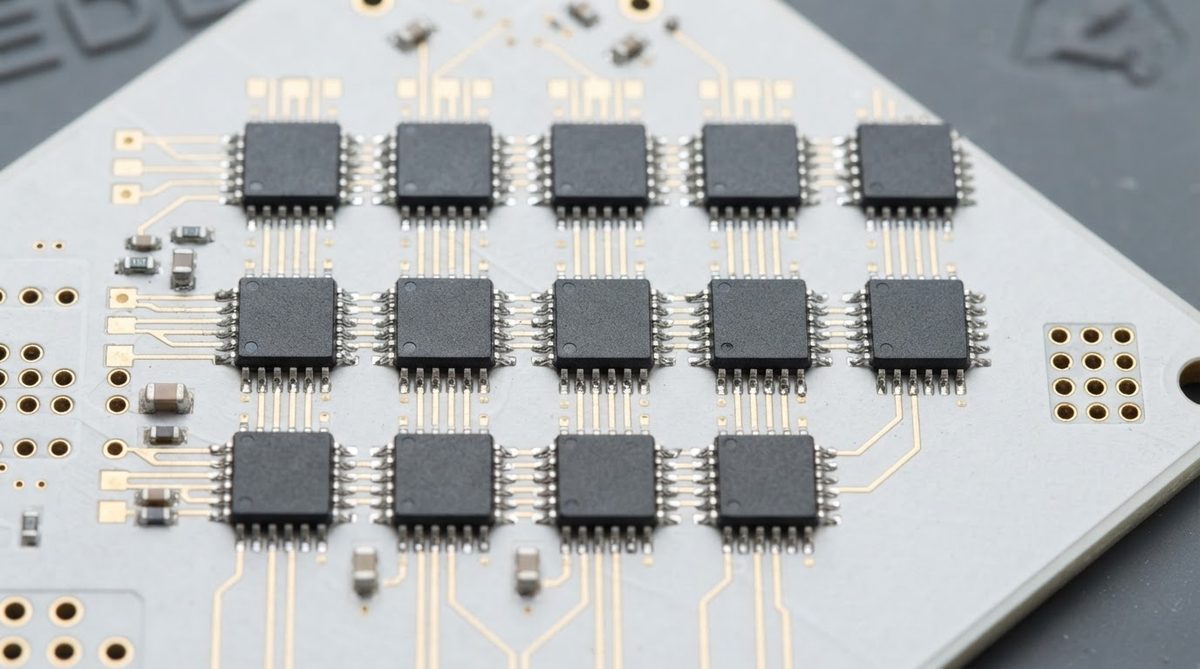
Suppose you have a 25 × 25 × 0.635 mm 96% alumina substrate with 12 QFN-16 packages, reflowed with SAC305 paste. Here is how to set the initial profile:
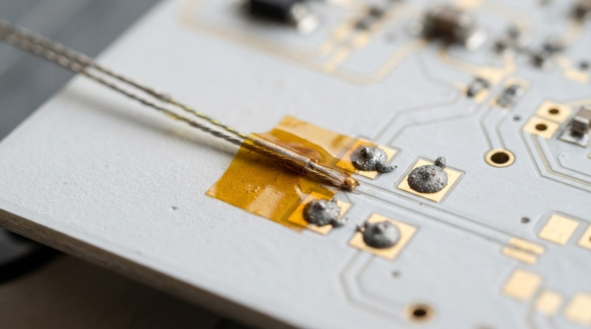
- Attach thermocouples. Place one on the bare ceramic surface at the board center, one on a corner pad, and one on the largest component body. Use Kapton tape or high-temp adhesive, not solder, to avoid altering the thermal mass at the measurement point.
- Set preheat ramp at 2.0 °C/s. The board mass is small (≈ 1.5 g ceramic + ~0.3 g copper), so a moderate ramp is safe. For a larger 50 × 50 mm panel, drop to 1.5 °C/s.
- Soak at 160–190 °C for 90 s. This equalises the board. Watch the ΔT between center and corner thermocouples. If it exceeds 10 °C at the end of soak, extend the soak by 15 s increments.
- Ramp to 248 °C peak at 2.0 °C/s. The air temperature in the oven will need to be roughly 260–265 °C to drive the ceramic surface to 248 °C. This is oven-dependent; always trust the board thermocouple.
- Hold TAL at 80 s. Start conservative. If cross-sections show incomplete wetting or grainy joints, increase TAL by 10 s.
- Cool at 2.5 °C/s. If your oven cooling zone cannot achieve this, consider opening the exit door partially or adding a gentle nitrogen curtain. Do not use forced air blasts directly on the ceramic.
After the first run, cross-section at least two joints. Look for voiding above 25% (per IPC-7095D Class 3 limits) and any interfacial cracks between the solder fillet and the metallised pad. If you see cracks, slow the cooling rate first.
Setting Up a Profile: Use the Reflow Profile Builder
Enter your substrate material, board dimensions, paste alloy, and target peak temperature to generate a starting reflow profile that follows J-STD-020E guidelines for ceramic assemblies.
[pcb_calc type=”reflow-profile”]
Common Failure Modes from Wrong Profiles
Thermal shock cracking
Ceramic substrates have low fracture toughness: 3.5–4.0 MPa·√m for 96% alumina (per CoorsTek ADS-996), compared to FR-4 which simply delaminates rather than cracking. A ramp rate above 4 °C/s on a 1.0 mm alumina board can nucleate cracks from existing edge flaws. Silicon nitride substrates are tougher (6–8 MPa·√m) and tolerate faster ramps, but cost significantly more.
Cold joints from insufficient TAL
Because the ceramic wicks heat away from the solder interface, paste at the board center may spend only 30–40 s above 217 °C on a profile tuned for FR-4. The result is dull, grainy joints with poor shear strength. Extending soak time and raising peak temperature by 5–8 °C usually resolves this without increasing the risk of component damage.
Pad delamination
Thick-film metallisation on alumina (typically a glass-frit bonded Ag or AgPd layer) can delaminate if the cooling rate creates excessive shear stress at the metal-ceramic interface. Thin-film and DPC metallisation are more resistant because the adhesion mechanism is different (sputtered Ti/Cu vs. glass frit). Check your substrate metallisation type and its peel strength rating before finalising the cooling segment.
When NOT to Adjust: Standard FR-4 Profiles Are Fine
If your board is FR-4, metal-core aluminium (MCPCB), or a flex-rigid polyimide stack, a standard IPC-recommended SAC305 profile (per J-STD-020E) works without the modifications described here. The adjustments above apply specifically to bare ceramic and ceramic-on-metal (DBC, AMB) substrates where thermal conductivity exceeds ~10 W/mK and CTE drops below ~10 ppm/°C. If your design uses an MCPCB with a ceramic-filled dielectric layer, you are still reflowing onto an organic dielectric, and a standard profile is the correct starting point.
Rework Considerations
Ceramic boards can be reflowed multiple times, but each cycle accumulates thermal fatigue at the metallisation interface. Most thick-film alumina substrates tolerate 3–5 reflow cycles before adhesion degrades measurably. For detailed guidance on removing and replacing components, see the guide on reworking ceramic PCB assemblies.
Die Attach vs. SMT Reflow
If your ceramic board carries bare die rather than packaged SMT components, the thermal profile changes significantly. Die attach processes (eutectic AuSn, sintered silver, epoxy) use different temperature ranges and dwell times. The die attach process guide for ceramic substrates covers those profiles separately.
Frequently Asked Questions
Can I use the same reflow oven for ceramic and FR-4 boards?
Yes. The oven hardware is identical. You only need a different stored recipe with adjusted zone temperatures, belt speed, and cooling settings. Most modern reflow ovens with 8+ zones can handle both by switching profiles.
Does lead-free paste work on ceramic substrates?
SAC305 and other lead-free alloys work well on ceramic, provided the metallisation is compatible (ENIG, ENEPIG, or bare copper with OSP). The higher peak temperatures required for lead-free are well within the ceramic’s capability; alumina is stable to over 1,600 °C.
How many reflow cycles can a ceramic PCB withstand?
The ceramic itself is unaffected by repeated reflow. The limiting factor is the metallisation adhesion. Thick-film silver on alumina typically tolerates 3–5 cycles. Thin-film (sputtered) metallisation and DBC copper can handle 5–10 cycles without measurable peel-strength loss, per published reliability data from Heraeus and DuPont thick-film datasheets.
Should I use nitrogen atmosphere for ceramic reflow?
Nitrogen is recommended but not always required. It reduces oxidation of exposed copper pads and improves wetting, especially on fine-pitch components. For boards with bare copper metallisation and no surface finish, nitrogen (below 500 ppm O₂) is strongly recommended. For ENIG-finished boards, air reflow is usually acceptable.
What happens if I cool a ceramic board too fast?
Cooling faster than 4 °C/s on alumina can cause micro-cracks at solder joints due to the CTE mismatch between solder (~21 ppm/°C) and substrate (~7 ppm/°C). In extreme cases, the substrate itself can fracture from edge flaws propagating under thermal stress. Keep cooling below 3 °C/s as a safe default.