An ENIG finish deposits 3–6 µin (0.05–0.15 µm) of gold over 120–240 µin (3–6 µm) of electroless nickel onto copper pads. On ceramic PCBs, the ENIG finish serves the same purpose as on FR-4—flat, coplanar, oxidation-resistant pads—but the ceramic substrate introduces differences in adhesion preparation, thermal cycling stress, and allowable process chemistry that engineers need to account for.
Key Takeaways
- The ENIG finish on ceramic PCBs follows IPC-4552B, targeting 3–6 µin Au and 120–240 µin Ni, the same spec as on organic boards.
- The nickel layer is the actual solder-joint interface; gold dissolves into the solder during reflow within seconds.
- Black pad (hyper-corrosion of the nickel surface) remains the primary reliability risk and is controlled through phosphorus content (8–12 wt% mid-phos Ni) and tight bath monitoring.
- An ENIG finish is compatible with both SAC305 reflow and gold or aluminum wedge/ball wire bonding, though thick-gold alternatives outperform it for high-reliability wire bonds.
- Ceramic substrates require a pre-treatment step (often a zincate or palladium activation) that differs from the oxide-etch used on FR-4 copper.
How the ENIG Finish Is Applied to a Ceramic PCB
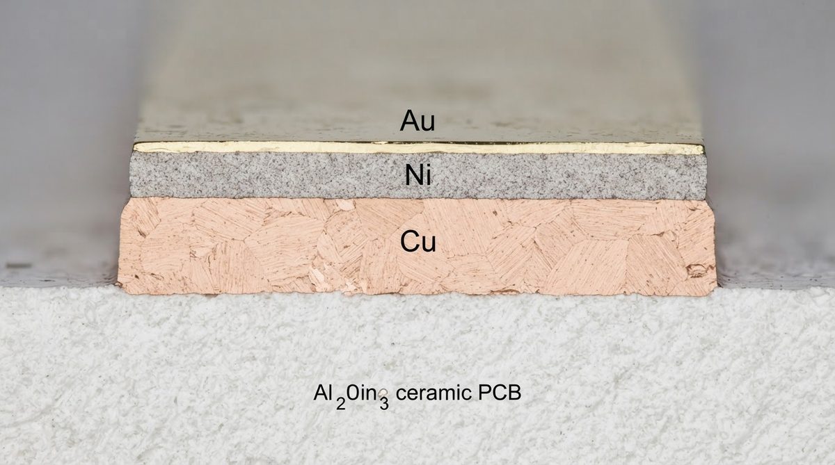
On an organic board, the copper surface is micro-etched to promote nickel adhesion. Ceramic PCBs with metallized pads (DPC sputtered copper, thick-film printed copper, or DBC bonded copper) need a different preparation. DPC copper is thin—typically 1–10 µm—so aggressive micro-etching risks exposing the titanium or chromium adhesion layer beneath. Fabricators use a mild acid clean followed by a palladium-based activator or a double-zincate process to catalyse electroless nickel deposition without removing significant copper.
After activation, the board enters the electroless nickel bath (typically a nickel-hypophosphite chemistry at 80–90 °C). Nickel deposits at roughly 15–25 µm/hr. Once the target thickness is reached, the board moves to the immersion gold bath, where a galvanic displacement reaction replaces a few atomic layers of nickel with gold. The gold layer is self-limiting: once it fully covers the nickel, the displacement reaction stops. This is why immersion gold thickness is measured in micro-inches, not mils.
For a deeper look at how ceramic substrates are metallized before finishing, see the guide to ceramic PCB manufacturing.
ENIG Finish Specification Table for Ceramic PCBs
| Parameter | Value | Unit | Condition / Standard | Source |
|---|---|---|---|---|
| Gold thickness | 3–6 (0.05–0.15) | µin (µm) | Per IPC-4552B, Rev. B | IPC-4552B |
| Nickel thickness | 120–240 (3–6) | µin (µm) | Per IPC-4552B | IPC-4552B |
| Nickel phosphorus content | 8–12 | wt% | Mid-phos, per IPC-4552B | IPC-4552B |
| Surface roughness (Ni) | 0.1–0.5 | µm Ra | Measured post-gold | Typical process data |
| Solderable shelf life | 12+ | months | Stored per IPC J-STD-033D, ≤30 °C / 60% RH | IPC J-STD-033D |
| Max reflow cycles (Pb-free) | 5–6 | cycles | 260 °C peak, SAC305 | IPC-4552B / solder paste vendor data |
| Contact resistance | <10 | mΩ | Fresh surface, probe test | Typical |
Typical values for commercially available material, for comparison only. Confirm against the datasheet for your specific grade.
Why Engineers Choose an ENIG Finish for Ceramic Boards
Pad coplanarity. Electroless deposition follows the copper surface uniformly. There are no uneven peaks like HASL leaves behind. This matters for ceramic PCBs carrying fine-pitch QFN, BGA, or flip-chip components where pad height variation must stay within 10–15 µm.
Wire-bond compatibility. Gold ball bonding works directly on the ENIG finish gold surface. Aluminum wedge bonding also works, though bond pull strength is lower than on thick electrolytic gold (typically 5–8 gf on ENIG versus 8–12 gf on 0.5 µm+ electrolytic Au, per MIL-STD-883 Method 2011). For Class 3 aerospace or medical wire bonds, many engineers specify thicker immersion gold or electrolytic gold finishes instead.
Long shelf life. Gold does not oxidize. Boards with an ENIG finish can sit in stock for over a year and still solder reliably, which suits low-volume ceramic PCB production runs where boards may wait months before assembly.
Black Pad: The Known ENIG Finish Failure Mode
Black pad is a hyper-corrosion defect at the nickel-gold interface. During immersion gold deposition, if the nickel grain boundaries corrode preferentially, a dark, brittle nickel-phosphorus-rich layer forms. Solder joints on affected pads look normal after reflow but fracture at the nickel surface under mechanical or thermal stress. The joint fails as a flat, dark fracture—hence the name.
Black pad risk is managed, not eliminated. Key controls include keeping the nickel bath’s phosphorus content within the 8–12 wt% mid-phos window, limiting gold bath age and metal loading, and maintaining the immersion gold pH between 4.5 and 5.0. IPC-4552B tightened corrosion acceptance criteria compared to the original IPC-4552, and any fabricator quoting an ENIG finish should be running to Rev. B or later.
On ceramic PCBs specifically, the risk is neither higher nor lower than on FR-4—black pad is a bath chemistry issue, not a substrate issue. But because ceramic boards often go into high-reliability applications (power modules, RF assemblies, medical implants), the consequences of a black pad escape are more severe. Cross-sectional inspection per IPC-4552B Appendix A on coupon samples is standard practice for critical builds.
ENIG Finish Compared to Other Ceramic PCB Finishes
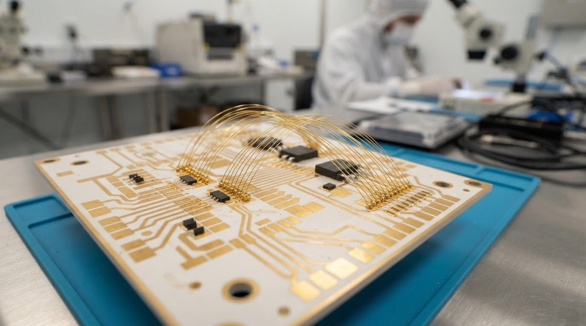
Use the tool below to compare an ENIG finish against other options based on your soldering method, shelf-life needs, and wire-bond requirements.
[pcb_calc type=”surface-finish”]
| Parameter | ENIG | ENEPIG | Immersion Ag | OSP |
|---|---|---|---|---|
| Typical Au thickness | 0.05–0.15 µm | 0.03–0.08 µm | N/A | N/A |
| Ni barrier layer | Yes (3–6 µm) | Yes (3–6 µm) | No | No |
| Pd layer | No | Yes (0.05–0.15 µm) | No | No |
| Wire-bond capable | Au ball, Al wedge | Au ball, Al wedge (better) | No | No |
| Black pad risk | Yes | Greatly reduced (Pd blocks corrosion) | N/A | N/A |
| Shelf life | 12+ months | 12+ months | 6–12 months | 3–6 months |
| Relative cost | Medium | High | Low–Medium | Low |
Typical values for commercially available material, for comparison only. Confirm against the datasheet for your specific grade.
For applications that need solderability but not wire bonding, immersion silver on ceramic substrates offers lower cost and avoids the black pad issue entirely. If oxidation protection is the only goal and shelf life is short, organic solderability preservative (OSP) is the simplest option.
When NOT to Use an ENIG Finish on a Ceramic PCB
High-reliability wire bonding (Class 3 / space-grade). The thin gold layer of an ENIG finish limits bond pull strength. Electrolytic gold or ENEPIG with thicker palladium provides a more reliable bonding surface for mission-critical wire bonds per MIL-STD-883.
Press-fit or high-insertion-cycle connectors. The nickel layer is hard (500–700 HV), which is good for contact wear. But the thin gold wears through after relatively few insertion cycles. Hard gold plating (0.5–1.5 µm electroplated Au over Ni) is the standard choice for connector fingers.
Cost-sensitive, short-shelf-life assemblies. If boards go straight to reflow within weeks and no wire bonding is needed, immersion tin or OSP costs less and solders just as well.
Aluminum-heavy wire bonding. Aluminum wedge bonds to an ENIG finish are acceptable but not optimal. The intermetallic formed between Al wire and the Ni underlayer (after gold dissolves) is less robust than Al-on-Al or Al-on-thick-Au. ENEPIG is the preferred compromise when both Al wire bonding and soldering are required on the same board.
Worked Example: Specifying an ENIG Finish for a Ceramic Power Module
Suppose you are designing a half-bridge SiC module on a 25 × 25 mm AlN DBC substrate. The top-side copper carries die-attach pads (reflowed with SAC305 at 260 °C peak) and wire-bond pads (gold ball bonds, 25 µm Au wire).
- Finish choice: ENIG finish per IPC-4552B. Specify 4–6 µin Au, 150–200 µin Ni, mid-phos (9–11 wt% P).
- Pre-treatment: Confirm with the fabricator that the DBC copper will receive a palladium activation rather than aggressive micro-etch, to preserve the Cu-ceramic bond.
- Wire-bond verification: Request 5 pull-test coupons per lot per MIL-STD-883 Method 2011. Accept criteria: ≥ 4.0 gf mean for 25 µm Au wire.
- Black pad screening: Require one cross-section per lot per IPC-4552B Appendix A. Nickel corrosion depth must not exceed 0.5 µm.
- Reflow budget: Allocate 3 reflow passes max (die attach, component reflow, rework allowance). The ENIG finish supports up to 5–6 cycles, leaving margin.
This specification set covers most ceramic power-module builds. For an overview of all available pad finishes and how they interact with ceramic substrates, see the ceramic PCB surface finish guide.
Frequently Asked Questions
Does an ENIG finish add significant thickness to ceramic PCB pads?
Total added thickness is roughly 3–6 µm (the nickel layer dominates). This is negligible for most designs but should be accounted for in ultra-fine-pitch flip-chip applications where pad coplanarity tolerances are under 10 µm.
Can I rework a ceramic board with an ENIG finish?
Yes. ENIG pads tolerate multiple reflow cycles (typically 5–6 at 260 °C peak). The gold dissolves into the solder on the first pass, so subsequent cycles are solder-to-nickel joints. Rework with a hot-air tool is standard. For more detail, see the guide on ceramic PCB rework.
Is an ENIG finish RoHS compliant?
Yes. An ENIG finish contains no lead, cadmium, mercury, or other RoHS-restricted substances. It is one of the standard Pb-free finishes across the industry.
What is the cost difference between ENIG and ENEPIG on ceramic?
ENEPIG typically costs 15–30% more than an ENIG finish per board, driven by the additional palladium bath step. The premium is justified when you need both soldering and aluminum wire bonding on the same substrate, or when black-pad risk must be minimized for Class 3 reliability.
Does the ceramic substrate affect ENIG finish adhesion?
The substrate itself does not contact the ENIG layers—nickel bonds to the copper metallization, not to the ceramic. However, the copper-to-ceramic adhesion method (DPC sputtering, DBC bonding, thick-film printing) determines how much copper is available for the ENIG pre-treatment. Thin DPC copper (1–3 µm) needs gentler chemistry than thick DBC copper (300 µm).
Next Step
If you have a ceramic PCB design that needs an ENIG finish or you are comparing finishes for a specific application, upload your files for a quick review and quote. The engineering team can confirm finish compatibility with your metallization and assembly process.