Most ceramic PCB substrates ship in thicknesses between 0.25 mm and 2.0 mm, with 0.381 mm (0.015″) and 0.635 mm (0.025″) accounting for the majority of production orders. The right thickness depends on your material, thermal path requirements, mechanical strength needs, and metallization process.
Standard Ceramic PCB Thickness Options by Material
Substrate manufacturers such as Kyocera, Maruwa, and CoorsTek produce ceramic blanks in a set of standard thicknesses. Custom thicknesses are possible but add cost and lead time because they require non-standard tape casting or grinding runs.
| Material | Common Thicknesses (mm) | Min Available (mm) | Max Available (mm) | Notes |
|---|---|---|---|---|
| Al₂O₃ 96% | 0.25, 0.381, 0.50, 0.635, 1.0 | 0.10 | 2.0 | Widest range; most stock options |
| Al₂O₃ 99.6% | 0.25, 0.381, 0.635 | 0.15 | 1.5 | Tighter thickness tolerance than 96% |
| AlN | 0.381, 0.635, 1.0 | 0.25 | 1.5 | Thinner blanks are fragile; handle with care |
| Si₃N₄ | 0.32, 0.635 | 0.20 | 1.0 | Highest flexural strength; allows thinner use |
| ZrO₂ (zirconia) | 0.10, 0.20, 0.30 | 0.05 | 0.50 | Used mainly in ultra-thin sensor substrates |
Typical values for commercially available material, for comparison only. Confirm against the datasheet for your specific grade.
How Thickness Affects Thermal and Mechanical Performance
Thermal resistance through the substrate scales linearly with thickness. For a simple one-dimensional path: Rth = t / (k × A), where t is thickness in meters, k is thermal conductivity in W/m·K, and A is the heat-spreading area in m². Halving the substrate thickness halves the conduction resistance.
Worked example: A 10 mm × 10 mm 96% alumina substrate (k ≈ 25 W/m·K) at 0.635 mm thick gives Rth = 0.000635 / (25 × 0.0001) = 0.254 °C/W. Switching to 0.381 mm drops that to 0.152 °C/W — a meaningful reduction for a power device dissipating several watts.
Thinner substrates are more fragile, though. Al₂O₃ 96% has a flexural strength of roughly 350–380 MPa (per ASTM C1161), which is adequate at 0.381 mm for most pick-and-place and reflow processes. AlN is weaker at around 300–350 MPa, so going below 0.381 mm requires careful handling fixtures. Si₃N₄, with flexural strength above 650 MPa, tolerates thinner profiles with less breakage risk.
Enter your substrate material, area, and layer count below to see how thickness changes your total board profile and estimated thermal resistance.
[pcb_calc type=”stackup-thickness”]
Choosing the Right Thickness for Your Design
Start with the thermal budget. If conduction through the substrate is your dominant thermal resistance, go as thin as your handling and assembly process allows. For most SMT lines, 0.381 mm Al₂O₃ or AlN is the practical minimum without custom fixtures.
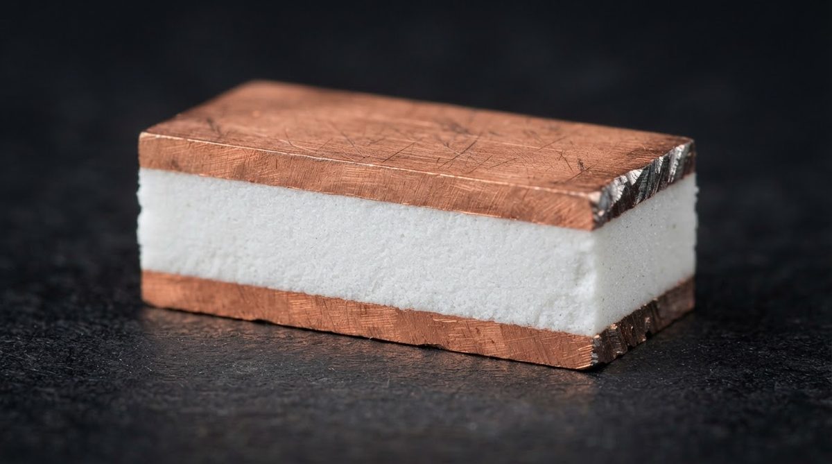
If the board must survive mechanical shock or clamping forces — common in automotive power modules — thicker substrates (0.635 mm to 1.0 mm) add margin. DBC and AMB substrates typically use 0.381 mm or 0.635 mm ceramic cores with bonded copper on both sides; the copper layers add stiffness, so the ceramic itself can stay thin.
For RF and microwave circuits, thickness sets the impedance of microstrip lines. A 0.254 mm Al₂O₃ 99.6% substrate (εr ≈ 9.9) gives a 50 Ω microstrip width of roughly 0.24 mm — convenient for fine-pitch layouts. Doubling the substrate thickness doubles the required trace width, which may conflict with dense routing.
When a Ceramic Substrate Is the Wrong Choice

If your design needs a thickness above 2.0 mm, ceramic substrates become impractical; consider an aluminum MCPCB or a copper heat sink with a thin ceramic isolator bonded on top. For boards thicker than 3.2 mm with many through-hole components, standard FR-4 is cheaper and easier to drill. And if cost is the primary driver on a low-power consumer board, the price premium of ceramic over FR-4 rarely justifies itself regardless of thickness. See the frequently asked questions on ceramic PCBs for more on where ceramic does and does not make sense.
FAQ
What is the thinnest ceramic PCB you can get?
Zirconia (ZrO₂) substrates are available down to 0.05 mm (50 µm). For alumina, the practical minimum is about 0.10 mm, though 0.25 mm is far more common in circuit production. Handling and metallization become the limiting factors at extreme thinness.
Does ceramic PCB thickness affect dielectric breakdown voltage?
Yes. Breakdown voltage increases roughly in proportion to thickness. Al₂O₃ 96% has a dielectric strength of about 10–15 kV/mm (per IEC 60672), so a 0.635 mm substrate withstands approximately 6–10 kV. Thinner substrates require derating for high-voltage isolation.
Can I get a custom thickness not listed as standard?
Yes, but expect a minimum-order quantity for the raw substrate blanks and longer lead times. The ceramic is produced by tape casting in specific thicknesses, and non-standard values require a dedicated casting or a grinding step after sintering.
How tight is the thickness tolerance on ceramic substrates?
Standard tolerance is typically ±0.05 mm for as-fired substrates and ±0.025 mm or better for ground (lapped) substrates, per manufacturer datasheets from Kyocera and Maruwa. Ground finishes cost more but are necessary when thickness uniformity affects impedance control or thermal interface resistance.
Is a thicker ceramic PCB always stronger?
A thicker substrate resists bending loads better because the moment of inertia increases with the cube of thickness. However, the intrinsic flexural strength of the material (in MPa) does not change. A 1.0 mm ceramic PCB tolerates higher applied force before fracture, but it is no less brittle than a 0.381 mm one of the same grade.