Yes, you can solder to a ceramic PCB. Solder wets to the metallized pads on the substrate — copper, silver, gold, or tungsten — not to the bare ceramic itself. With the right metallization, solder alloy, and reflow profile, ceramic PCB joints are as reliable as those on FR-4, and often more so at high temperatures.
The critical difference is that ceramic is brittle. It does not flex to absorb thermal stress the way an organic laminate does. That means your solder choice, pad design, and reflow ramp rate all matter more than usual. If you are asking “can you solder to ceramic PCB” for the first time, the short answer is yes — the longer answer is about controlling the details that follow.
Why Bare Ceramic Won’t Take Solder
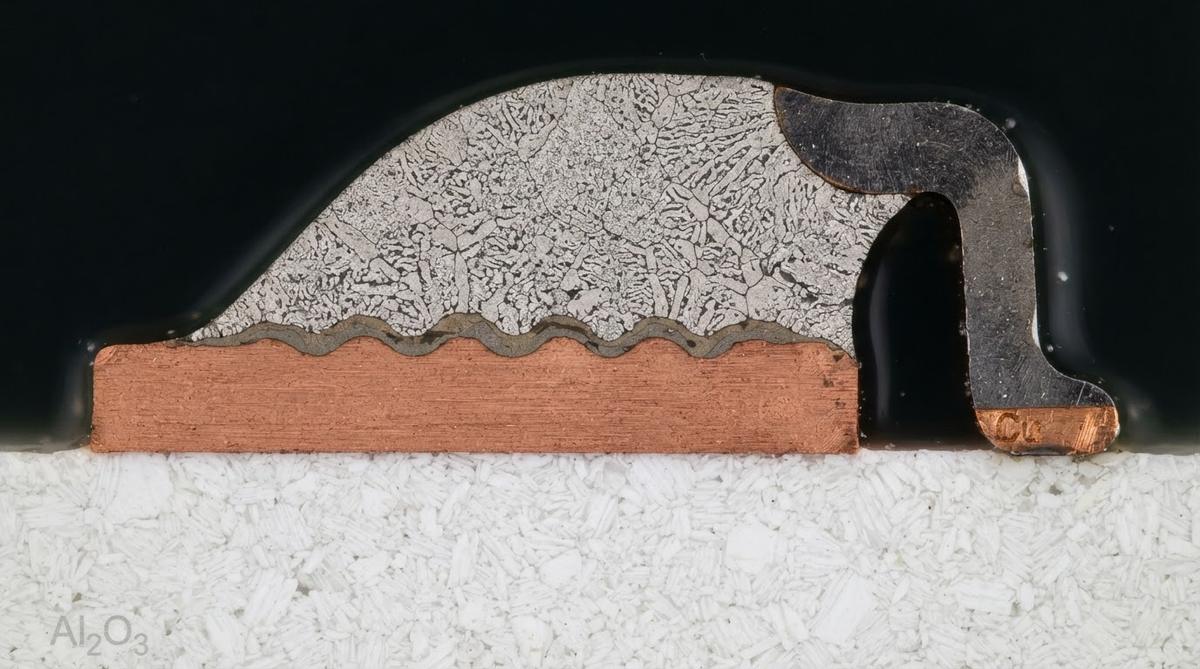
Alumina (Al₂O₃), aluminum nitride (AlN), and silicon nitride (Si₃N₄) are oxide or nitride ceramics. Their surfaces are chemically inert and non-wettable by tin-based solders. No amount of flux will make SAC305 bond directly to a polished alumina face. You need an intermediate metal layer — the metallization — that bonds to the ceramic on one side and accepts solder on the other.
This is why every solderable ceramic circuit board ships with patterned metal already applied. The metallization method determines what solders you can use and how strong the joint will be.
Can You Solder to Ceramic PCB with Any Metallization?
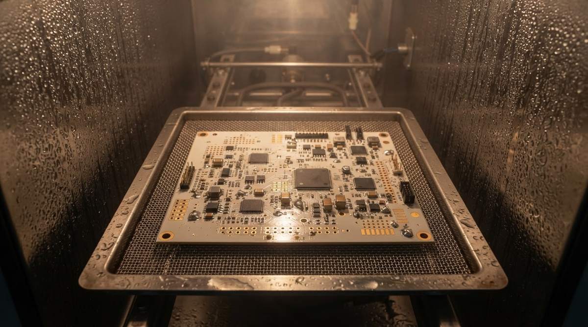
Different ceramic PCB processes produce different pad metals. Each has its own soldering characteristics, and not all are equal in wettability or joint strength.
| Metallization | Typical Metal Stack | Compatible Solders | Notes |
|---|---|---|---|
| DPC (Direct Plated Copper) | Ti/Cu seed + electroplated Cu (up to ~100 µm), often with Ni/Au finish | SAC305, SnPb, SnBi, AuSn | Excellent wettability; fine-pitch capable |
| DBC (Direct Bonded Copper) | Cu foil (127–635 µm) bonded via Cu₂O eutectic | SAC305, SnPb, high-Pb, AuSn, sintered Ag | Thick copper; used in power modules |
| AMB (Active Metal Brazing) | Cu foil brazed with AgCuTi | SAC305, SnPb, high-Pb, sintered Ag | Strongest ceramic-to-copper bond; suits AlN and Si₃N₄ |
| Thick Film (Ag, AgPd, Au) | Screen-printed Ag or AgPd (8–15 µm), fired at 850 °C | SAC305, SnPb, SnBi | Ag leaching risk — use Ag-bearing solder or barrier Ni plate |
| Thin Film (sputtered) | TiW/Au or Cr/Ni/Au (0.5–5 µm total) | AuSn, SAC305, SnPb | Best for RF and fine-pitch; delicate — avoid aggressive fluxes |
| HTCC (co-fired W or Mo) | Tungsten or moly-manganese, Ni/Au plated | SAC305, SnPb, AuSn | Ni barrier is essential for solderability |
Typical values for commercially available material, for comparison only. Confirm against the datasheet for your specific grade.
Which Solder Alloys Work on Ceramic Substrates
Any standard electronics solder can wet properly metallized ceramic pads. The real question is which alloy best handles the CTE mismatch between ceramic and the component being attached.
Alumina 96% has a CTE of about 7.1 ppm/°C (per CoorsTek datasheet, 25–300 °C). AlN sits near 4.5 ppm/°C. Silicon dies are around 2.6 ppm/°C, and copper lead frames are roughly 17 ppm/°C. The solder joint must survive the shear stress caused by these differences through every thermal cycle. Understanding ceramic thermal management principles helps you pick the right alloy for your operating range.
For detailed alloy recommendations, see the guide on solder and paste selection for ceramic boards. A quick summary:
- SAC305 (Sn96.5/Ag3.0/Cu0.5): The default lead-free choice. Liquidus 217–220 °C. Works well for most SMD assembly on ceramic.
- Sn63/Pb37: Still used in mil/aero and medical where RoHS exemptions apply. Liquidus 183 °C. Lower stress on joints due to lower reflow temperature.
- AuSn (Au80/Sn20): Eutectic at 280 °C. Fluxless soldering in inert atmosphere. Standard for hermetic packages and die attach on thin-film ceramic.
- High-Pb (Pb92.5/Sn5/Ag2.5): Liquidus ~300 °C. Used in power module die attach where the joint must survive a second reflow without re-melting.
- Sintered silver: Not a solder, but increasingly common on DBC and AMB substrates for SiC die attach. Withstands 300 °C+ continuous operation.
Enter your substrate material, component CTE, and operating temperature range to see how thermal cycling affects joint strain over time.
Reflow Profile Considerations for Ceramic
Ceramic substrates have low thermal mass per unit area compared to thick FR-4 multilayers, so they heat faster. At the same time, ceramic is brittle and sensitive to thermal shock. These two facts shape your reflow profile — and they are central to whether you can solder to ceramic PCB assemblies without damage.
Ramp Rate
Keep the ramp below 3 °C/s. A sudden temperature gradient across a 0.635 mm alumina substrate can generate enough tensile stress on the cooler face to initiate a crack. Per ASTM C1161, the flexural strength of 96% alumina is 345–380 MPa, but micro-flaws from laser scribing or edge grinding can lower the effective strength. A conservative ramp — 1.5 to 2.5 °C/s — costs you a few seconds and eliminates the risk.
Peak Temperature and Time Above Liquidus
Follow the solder manufacturer’s recommendation. For SAC305, a peak of 240–250 °C with 60–90 s above 217 °C is typical. On thick-film silver pads without a nickel barrier, minimize time above liquidus to limit silver leaching — 45 s is a practical upper bound.
Cooling
Controlled cooling at 2–4 °C/s is fine. Avoid quenching or forced-air cooling directly on the ceramic face. Uneven cooling creates the same thermal gradient problem as aggressive ramp-up.
Worked Example: Thermal Stress on a Solder Joint
Suppose you solder a 5 × 5 mm copper lead frame (CTE ≈ 17 ppm/°C) to a 96% alumina substrate (CTE ≈ 7.1 ppm/°C) using SAC305. The joint cools from 220 °C to 25 °C — a ΔT of 195 °C.
CTE mismatch: 17 − 7.1 = 9.9 ppm/°C. Differential strain over the diagonal of the pad (≈ 7.07 mm): 9.9 × 10⁻⁶ × 195 × 7.07 mm ≈ 0.0137 mm, or about 13.7 µm. For a solder joint height of 75 µm (typical BGA standoff), the shear strain is 13.7 / 75 ≈ 0.18, or 18%. That is high. Fatigue life drops sharply above ~10% shear strain per the Coffin-Manson model.
Practical fixes: use a thicker solder joint (150 µm standoff halves the strain), add an underfill, or switch to a CTE-matched component carrier. This kind of calculation is why power module designers pair ceramic substrates with bare dies (CTE 2.6–4.5 ppm/°C for Si/SiC) rather than packaged parts with copper lead frames.
Common Mistakes When Soldering Ceramic PCBs
- Skipping bake-out on thick-film boards. Thick-film pastes are porous. Moisture absorbed during storage can cause solder spattering. Bake at 125 °C for 2–4 hours before reflow. Check ceramic PCB storage and shelf life guidelines for recommended conditions.
- Using no-clean flux on thin-film metallization. Residues can corrode thin sputtered layers. Use a rosin-based or water-soluble flux and clean after reflow.
- Clamping the substrate too tightly in a fixture. Ceramic does not yield. A rigid clamp plus thermal expansion equals a cracked board. Use compliant pads or spring-loaded fixtures.
- Ignoring silver leaching. On thick-film Ag pads, standard SAC305 dissolves silver at roughly 0.5–1.0 µm per second above liquidus. Either plate Ni over the Ag or use a solder with 2–3% Ag content to slow the dissolution.
When Soldering Is Not the Right Attachment Method
Even though you can solder to ceramic PCB substrates in most cases, there are situations where another method is better:
- Continuous operation above 300 °C: Standard solders re-melt or creep. Use sintered silver, gold-germanium brazing, or epoxy die attach rated for the temperature. See ceramic PCB max operating temperature for limits by material.
- Bare die on unmetallized ceramic: Use conductive epoxy or eutectic die attach, not solder.
- Large-area bonding (>25 × 25 mm) with high CTE mismatch: The accumulated shear strain can exceed solder fatigue limits within hundreds of cycles. Consider a compliant interface layer or mechanical fastening with thermal grease.
- Ultra-fine pitch below 100 µm: Wire bonding or flip-chip with thermocompression may give better yield than solder paste printing at that scale.
If your application is better served by an organic laminate or a metal-core board, ceramic is not the right substrate — and that is a perfectly valid conclusion.
Hand Soldering vs. Reflow vs. Vapor Phase
Hand soldering with a temperature-controlled iron works for prototypes and rework. Use a chisel tip, keep the iron at 350–370 °C for SAC305, and do not press down on the substrate. Ceramic does not absorb shock the way FR-4 does. A slip can chip the edge or crack a thin board.
Reflow (convection or IR) is the standard production method. Vapor-phase reflow is particularly well-suited to ceramic because the condensation heating is inherently uniform — no hot spots from IR absorption differences between metal and ceramic surfaces. The maximum temperature is fixed by the fluid’s boiling point (e.g., 230 °C for Galden LS230), which prevents overshoot.
For step-by-step soldering procedures, see the full guide on how to solder a ceramic PCB.
Frequently Asked Questions
Can I use a standard SMT pick-and-place line for ceramic PCBs?
Yes. Ceramic PCBs run through standard pick-and-place and reflow equipment with no modifications. The main adjustment is the reflow profile — slower ramp rates to protect the brittle substrate. Tooling rails or custom carriers may be needed if the board is smaller than the machine’s minimum panel size.
Does ceramic PCB thickness affect soldering?
Thinner substrates (0.25–0.38 mm) heat faster and are more fragile, so they need gentler handling and slower ramp rates. Thicker boards (0.635–1.0 mm) behave more like standard PCBs in reflow. See available options on the ceramic PCB thickness page.
Will wave soldering work on ceramic?
It can, but it is rarely used. The thermal shock of contacting a 260 °C solder wave risks cracking the substrate. If through-hole components are required, selective soldering with preheating is safer than a full wave process.
Do I need a special stencil for solder paste on ceramic?
No special stencil material is needed. Use a laser-cut stainless steel stencil sized to your pad geometry, just as you would for FR-4. For thick-film silver pads, reduce the aperture by 10–15% to limit paste volume and silver leaching.
Can I rework a component on a ceramic PCB?
Yes. Use a focused hot-air rework station. Preheat the board to 100–150 °C to reduce thermal shock, then apply localized heat to the joint. Avoid mechanical prying — a spudger slipping off a pad can chip the ceramic edge.