Introduction to PCB Via
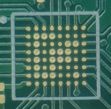
A PCB (Printed Circuit Board) via is a small hole drilled through a PCB to allow electrical connections between different layers of the board. Vias are essential components in multi-layer PCBs, enabling the routing of signals and power between layers, thus minimizing the board size and increasing the design flexibility.
Types of PCB Vias
There are several types of PCB vias, each with its own characteristics and applications:
-
Through-hole Vias
- Drilled through the entire thickness of the PCB
- Provide electrical connection between all layers
-
Suitable for components with through-hole mounting
-
Blind Vias
- Drilled from one surface of the PCB to an internal layer
- Not visible on the opposite surface
-
Used for connecting outer layers to inner layers
-
Buried Vias
- Drilled between internal layers of the PCB
- Not visible on either surface of the board
-
Used for connecting inner layers to each other
-
Micro Vias
- Smaller in size compared to other via types
- Typically used in high-density interconnect (HDI) PCBs
- Enable higher routing density and smaller form factors
| Via Type | Drilled From | Drilled To | Visibility |
|---|---|---|---|
| Through-hole | Top surface | Bottom surface | Both surfaces |
| Blind | One surface | Internal layer | One surface |
| Buried | Internal layer | Internal layer | No surface |
| Micro | One surface | Internal layer (HDI) | One surface |
Manufacturing Process of PCB Vias
The manufacturing process of PCB vias involves several steps:
-
Drilling
- Holes are drilled through the PCB using a CNC drilling machine
- Drill bit size determines the via diameter
-
Laser drilling is used for smaller vias (e.g., micro vias)
-
Plating
- The drilled holes are plated with a conductive material, usually copper
- Electroless copper plating is used to create a thin conductive layer
-
Electroplating is then used to build up the copper thickness
-
Filling (optional)
- Some vias may be filled with a non-conductive material (e.g., epoxy)
-
Via filling improves the structural integrity and facilitates component placement
-
Capping (optional)
- Via caps are used to cover the via openings on the PCB surface
- Capping enhances the PCB’s appearance and protects the vias from contamination

Design Considerations for PCB Vias
When designing PCBs with vias, several factors should be considered:
-
Via Size
- Choose the appropriate via size based on the PCB Thickness and layer count
-
Smaller vias allow for higher routing density but may increase manufacturing costs
-
Via Placement
- Place vias strategically to minimize the impact on signal integrity
-
Avoid placing vias in high-speed signal paths or under sensitive components
-
Via Pitch
- Maintain sufficient spacing between vias to ensure manufacturability
-
Follow the manufacturer’s guidelines for minimum via pitch
-
Via Stubs
- Minimize via stubs (unused portion of the via) to reduce signal reflections
- Use back-drilling or buried vias to remove or shorten via stubs

Signal Integrity Considerations
PCB vias can impact signal integrity, especially in high-speed designs:
-
Impedance Discontinuities
- Vias introduce impedance discontinuities due to the change in geometry
-
Minimize the via diameter and length to reduce the discontinuity
-
Capacitive and Inductive Effects
- Vias exhibit capacitive and inductive behavior at high frequencies
-
Use ground vias near signal vias to provide a return path and reduce crosstalk
-
Via Stubs
- Via stubs act as unterminated transmission lines, causing signal reflections
- Remove or shorten via stubs to minimize the impact on signal quality

Thermal Management and Vias
PCB vias play a role in thermal management by providing a path for heat dissipation:
-
Thermal Vias
- Used to transfer heat from components to other layers or heatsinks
- Placed under or near power-dissipating components
-
Filled with a thermally conductive material (e.g., solder or thermally conductive epoxy)
-
Via Arrays
- Multiple vias arranged in an array to increase the heat transfer surface area
-
Used in conjunction with thermal pads or heatsinks
-
Via-in-Pad
- Vias placed directly in the component pad to enhance heat dissipation
- Requires precise manufacturing control to avoid Solder wicking or component tilting
Advanced Via Techniques
Several advanced via techniques are used in modern PCB designs:
-
Via-in-Pad Plating
- Selective plating of vias in component pads
-
Allows for higher component density and improved thermal management
-
Copper-filled Vias
- Vias filled with copper instead of non-conductive material
- Provides better electrical and thermal conductivity
-
Improves structural integrity and reduces the risk of via failure
-
Stacked Vias
- Multiple vias stacked on top of each other to span multiple layers
-
Used when a single via cannot reach the desired layer due to depth limitations
-
Blind and Buried Via Stacking
- Combination of blind and buried vias to create complex interconnections
- Enables higher layer counts and increased design flexibility
Frequently Asked Questions (FAQ)
-
Q: What is the difference between a through-hole via and a blind via?
A: A through-hole via is drilled through the entire thickness of the PCB, connecting all layers. A blind via, on the other hand, is drilled from one surface of the PCB to an internal layer and is not visible on the opposite surface. -
Q: Why are micro vias used in PCB design?
A: Micro vias are used in high-density interconnect (HDI) PCBs to enable higher routing density and smaller form factors. They are smaller in size compared to other via types, allowing for more compact designs. -
Q: What is the purpose of via filling?
A: Via filling is the process of filling a via with a non-conductive material, such as epoxy. It improves the structural integrity of the PCB and facilitates component placement by providing a flat surface. -
Q: How do vias impact signal integrity in high-speed designs?
A: Vias can introduce impedance discontinuities, capacitive and inductive effects, and signal reflections due to via stubs. These factors can degrade signal quality in high-speed designs. Proper via design and placement, along with techniques like ground vias and back-drilling, can help mitigate these issues. -
Q: What are thermal vias, and how do they help with thermal management?
A: Thermal vias are used to transfer heat from power-dissipating components to other layers or heatsinks. They are placed under or near the components and are often filled with a thermally conductive material. Thermal vias help improve heat dissipation and prevent component overheating.
Conclusion
PCB vias are essential components in multi-layer PCB design, enabling electrical connections between different layers and allowing for more compact and flexible layouts. Understanding the types of vias, their manufacturing process, and design considerations is crucial for creating reliable and high-performance PCBs.
When designing with vias, it is important to consider factors such as via size, placement, pitch, and the impact on signal integrity. Advanced techniques like via-in-pad plating, copper-filled vias, and stacked vias offer additional options for optimizing PCB designs.
By carefully selecting the appropriate via types and implementing best practices for via design and manufacturing, engineers can create PCBs that meet the demanding requirements of modern electronic devices while ensuring reliability, signal integrity, and optimal thermal management.


Leave a Reply