Table of Contents
- Introduction to PCB Etching
- PCB Etching Methods
- Wet Chemical Etching
- Dry Etching
- The PCB Etching Process
- Step 1: PCB Design and Preparation
- Step 2: Applying the Etch Resist
- Step 3: Etching the PCB
- Step 4: Removing the Etch Resist
- Step 5: Inspection and Quality Control
- Factors Affecting PCB Etching Quality
- Etchant Type and Concentration
- Etching Time and Temperature
- Agitation and Circulation
- Etch Resist Quality
- Advantages and Disadvantages of PCB Etching Methods
- Environmental Considerations in PCB Etching
- Troubleshooting Common PCB Etching Issues
- Future Trends in PCB Etching Technology
- Frequently Asked Questions (FAQ)
- Conclusion
Introduction to PCB Etching
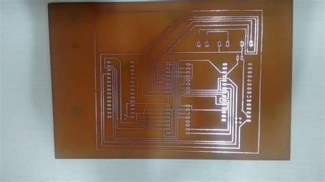
PCB etching is a subtractive process in which unwanted copper is removed from the surface of a copper-clad laminate, leaving behind the desired conductive patterns. This process is critical for creating the electrical connections between components on a PCB, ensuring proper functionality and reliability of the electronic device.
The etching process begins with a PCB design, which is transferred onto the copper surface using an etch resist. The etch resist protects the desired copper areas from the etching solution, while the unprotected areas are removed. The result is a PCB with the desired conductive patterns.

PCB Etching Methods
There are two primary methods for PCB etching: wet chemical etching and dry etching. Each method has its advantages and disadvantages, and the choice of method depends on factors such as the desired features, production volume, and environmental considerations.
Wet Chemical Etching
Wet chemical etching is the most common method for PCB etching. It involves immersing the PCB in an etching solution, typically an acidic or alkaline solution that reacts with the exposed copper, dissolving it and leaving behind the desired conductive patterns.
The most commonly used etchants in wet chemical etching are:
- Ferric Chloride (FeCl3)
- Cupric Chloride (CuCl2)
- Ammonium Persulfate ((NH4)2S2O8)
- Sodium Persulfate (Na2S2O8)
Wet chemical etching is relatively simple, cost-effective, and suitable for high-volume production. However, it has some limitations, such as the potential for undercut (widening of the etched features) and the need for proper waste management due to the use of hazardous chemicals.
Dry Etching
Dry etching, also known as plasma etching, is a more advanced method that uses reactive gases or vapors to remove the unwanted copper from the PCB surface. This method is performed in a vacuum chamber, where the PCB is exposed to a plasma containing the etching gases.
The most common dry etching techniques are:
- Reactive Ion Etching (RIE)
- Deep Reactive Ion Etching (DRIE)
- Ion Beam Etching (IBE)
Dry etching offers several advantages over wet chemical etching, such as higher precision, better control over the etching process, and the ability to create finer features. However, it is more expensive and requires specialized equipment, making it more suitable for low-volume production or high-end applications.

The PCB Etching Process
The PCB etching process consists of several steps, each of which plays a crucial role in achieving the desired outcome. Let’s take a closer look at each step.
Step 1: PCB Design and Preparation
The first step in the PCB etching process is designing the circuit using CAD (Computer-Aided Design) software. The design includes the layout of the conductive traces, component footprints, and other features. Once the design is finalized, it is transferred onto the copper surface of the PCB using an etch resist.
The most common methods for applying the etch resist are:
- Photoresist: A light-sensitive polymer that hardens when exposed to UV light. The PCB design is transferred onto the photoresist using a photomask and UV exposure.
- Silk Screen Printing: A stencil-based method where the etch resist is applied through a mesh screen onto the PCB surface.
- Laser Direct Imaging (LDI): A maskless method that uses a laser to directly transfer the PCB design onto the photoresist-coated PCB.
Step 2: Applying the Etch Resist
Once the PCB design is prepared, the etch resist is applied to the copper surface. The etch resist protects the desired copper areas from the etching solution, while the unprotected areas are removed during the etching process.
The application of the etch resist depends on the chosen method (photoresist, silk screen printing, or LDI). In the case of photoresist, the PCB is coated with the resist, exposed to UV light through a photomask, and then developed to remove the unexposed areas. This process creates a protective pattern on the copper surface that matches the desired PCB design.
Step 3: Etching the PCB
With the etch resist in place, the PCB is ready for etching. The etching process removes the unwanted copper from the unprotected areas, leaving behind the desired conductive patterns.
In wet chemical etching, the PCB is immersed in an etching solution, which reacts with the exposed copper, dissolving it. The etching time depends on factors such as the etchant type, concentration, temperature, and agitation. The process is carefully monitored to ensure proper etching and to avoid over-etching, which can lead to undercut and damage to the desired features.
In dry etching, the PCB is placed in a vacuum chamber and exposed to a plasma containing the etching gases. The plasma reacts with the exposed copper, removing it from the surface. The etching process is controlled by adjusting parameters such as gas flow, pressure, and power.
Step 4: Removing the Etch Resist
After etching, the etch resist is no longer needed and must be removed from the PCB surface. The removal process depends on the type of etch resist used.
For photoresist, a stripping solution (usually an alkaline solution) is used to dissolve the resist, leaving behind the clean, etched PCB. In the case of silk screen printing or other etch resists, a suitable solvent is used to remove the resist.
Step 5: Inspection and Quality Control
The final step in the PCB etching process is inspection and quality control. The etched PCB is thoroughly examined to ensure that the desired features are correctly formed, and there are no defects such as undercut, overetching, or short circuits.
Various inspection methods can be used, such as:
- Visual Inspection: A manual inspection using a microscope or magnifying glass to check for visible defects.
- Automated Optical Inspection (AOI): A computer-aided inspection that uses cameras and image processing algorithms to detect defects.
- Electrical Testing: A functional test that checks the electrical continuity and isolation of the PCB traces.
Any defects or issues identified during the inspection process are addressed, and the PCB is reworked or rejected if necessary.

Factors Affecting PCB Etching Quality
Several factors can influence the quality of the etched PCB. Understanding and controlling these factors is essential for achieving the desired results and minimizing defects.
Etchant Type and Concentration
The choice of etchant and its concentration play a significant role in the etching process. Different etchants have varying etching rates, selectivity, and compatibility with the PCB materials. The concentration of the etchant also affects the etching speed and the quality of the etched features.
For example, ferric chloride is a popular choice for wet chemical etching due to its high etching rate and good selectivity. However, it can cause undercut if the concentration is too high or the etching time is too long. On the other hand, cupric chloride has a lower etching rate but offers better control over the etching process, resulting in less undercut.
Etching Time and Temperature
The etching time and temperature are critical parameters that determine the speed and quality of the etching process. Higher temperatures and longer etching times generally result in faster etching rates but can also lead to overetching and undercut.
It is essential to optimize the etching time and temperature based on the specific PCB design, etchant type, and desired features. Proper control and monitoring of these parameters ensure consistent and reliable etching results.
Agitation and Circulation
Agitation and circulation of the etching solution are important factors in wet chemical etching. Proper agitation helps to maintain a uniform etchant concentration and temperature across the PCB surface, promoting even etching and reducing the risk of undercut.
Circulation of the etching solution also helps to remove the etching byproducts (such as copper salts) from the PCB surface, preventing them from interfering with the etching process and ensuring a clean and consistent etch.
Etch Resist Quality
The quality of the etch resist is another critical factor in PCB etching. A high-quality etch resist ensures proper protection of the desired copper areas, resulting in well-defined and accurate conductive patterns.
Poor-quality etch resists can lead to issues such as incomplete coverage, pinholes, or lifting during the etching process. These defects can cause unintended etching, short circuits, or open circuits, compromising the functionality and reliability of the PCB.
Advantages and Disadvantages of PCB Etching Methods
Each PCB etching method has its advantages and disadvantages. Understanding these factors can help in selecting the most suitable method for a given application.
Wet Chemical Etching:
– Advantages:
– Cost-effective and suitable for high-volume production
– Simple and easily scalable process
– Widely available materials and equipment
– Disadvantages:
– Potential for undercut and overetching
– Limited resolution and feature size
– Environmental and safety concerns due to hazardous chemicals
Dry Etching:
– Advantages:
– High precision and control over the etching process
– Ability to create fine features and high aspect ratios
– Reduced environmental impact compared to wet chemical etching
– Disadvantages:
– Higher cost and complexity compared to wet chemical etching
– Requires specialized equipment and skilled operators
– Limited throughput and more suitable for low-volume production
Environmental Considerations in PCB Etching
PCB etching involves the use of chemicals and generates waste that can have an environmental impact. It is essential to consider environmental factors and implement responsible practices to minimize the ecological footprint of the etching process.
Some key environmental considerations in PCB etching include:
- Proper handling, storage, and disposal of etching chemicals
- Treatment and recycling of etching waste (such as spent etchant and rinse water)
- Implementation of closed-loop systems to minimize chemical consumption and waste generation
- Use of alternative, environmentally friendly etchants (such as hydrogen peroxide or citric acid)
- Compliance with local and international environmental regulations and standards
By adopting environmentally responsible practices, PCB manufacturers can reduce their environmental impact and contribute to a more sustainable future.
Troubleshooting Common PCB Etching Issues
Despite careful control and optimization of the etching process, issues can still arise. Troubleshooting these issues is crucial for maintaining the quality and reliability of the etched PCBs.
Some common PCB etching issues and their possible causes include:
- Undercut: Overetching, high etchant concentration, or prolonged etching time
- Incomplete etching: Low etchant concentration, insufficient etching time, or poor agitation
- Etch resist lifting: Poor etch resist adhesion, incompatible etchant, or excessive agitation
- Rough or pitted copper surface: Contaminated etchant, inadequate cleaning, or improper etching conditions
To troubleshoot these issues, it is essential to systematically analyze the etching process, identify the root cause, and implement appropriate corrective actions. This may involve adjusting the etching parameters, improving the etch resist application, or optimizing the cleaning and inspection procedures.
Future Trends in PCB Etching Technology
As the demand for smaller, more complex, and high-performance PCBs continues to grow, the PCB etching technology is evolving to meet these challenges. Some of the future trends in PCB etching include:
- Adoption of advanced etching methods, such as laser etching or plasma etching, for high-precision and fine-feature applications
- Development of novel, environmentally friendly etchants and processes to reduce the environmental impact of PCB manufacturing
- Integration of artificial intelligence and machine learning techniques for process optimization and quality control
- Increased use of additive manufacturing techniques, such as 3D printing, in combination with etching for creating complex, three-dimensional PCB structures
These advancements in PCB etching technology will enable the production of more sophisticated and reliable PCBs, driving innovation in various industries, from consumer electronics to aerospace and beyond.
Frequently Asked Questions (FAQ)
- What is the difference between wet chemical etching and dry etching?
-
Wet chemical etching involves immersing the PCB in an etching solution, while dry etching uses reactive gases or vapors in a vacuum chamber to remove the unwanted copper. Wet chemical etching is more common and cost-effective, while dry etching offers higher precision and the ability to create finer features.
-
What are the most common etchants used in wet chemical etching?
-
The most common etchants used in wet chemical etching are ferric chloride (FeCl3), cupric chloride (CuCl2), ammonium persulfate ((NH4)2S2O8), and sodium persulfate (Na2S2O8). Each etchant has its advantages and disadvantages in terms of etching rate, selectivity, and compatibility with the PCB materials.
-
How can I minimize undercut during the PCB etching process?
-
To minimize undercut, you can optimize the etching parameters, such as the etchant concentration, etching time, and temperature. Using a high-quality etch resist and ensuring proper agitation and circulation of the etching solution can also help to reduce undercut.
-
What are the environmental concerns associated with PCB etching, and how can they be addressed?
-
PCB etching involves the use of hazardous chemicals and generates waste that can have an environmental impact. To address these concerns, proper handling, storage, and disposal of etching chemicals, as well as treatment and recycling of etching waste, are essential. Adopting environmentally friendly etchants and implementing closed-loop systems can also help to reduce the environmental footprint of PCB etching.
-
What are the future trends in PCB etching technology?
- Future trends in PCB etching technology include the adoption of advanced etching methods (such as laser etching or plasma etching), development of novel, environmentally friendly etchants and processes, integration of artificial intelligence and machine learning techniques for process optimization and quality control, and increased use of additive manufacturing techniques in combination with etching for creating complex, three-dimensional PCB structures.
Conclusion
PCB etching is a critical process in the manufacturing of printed circuit boards, enabling the creation of the desired conductive patterns that form the electrical connections between components. By understanding the methods, steps, and factors that influence the quality of the etched PCBs, manufacturers can optimize their processes to achieve consistent and reliable results.
As the electronics industry continues to evolve, so does the PCB etching technology. Advancements in etching methods, materials, and process control will drive the production of more sophisticated and high-performance PCBs, supporting innovation across various sectors.
By staying informed about the latest developments in PCB etching and adopting best practices for quality, efficiency, and environmental responsibility, PCB manufacturers can position themselves for success in an increasingly competitive and dynamic market.


Leave a Reply