Understanding Solder Escape and Its Impact on PCB Assembly
Solder escape, also known as solder wicking, is a common issue faced during the reflow soldering process in PCB assembly. It occurs when molten solder flows away from the intended joint and spreads along the surface of the PCB or component leads. This unwanted solder flow can lead to various problems, such as bridging between adjacent pads, insufficient solder joint formation, and reduced reliability of the assembLED PCB.
In this article, we will explore the causes of solder escape, its impact on PCB assembly, and provide practical tips and tricks to mitigate this issue during the reflow process.
Causes of Solder Escape
Several factors can contribute to the occurrence of solder escape during reflow soldering:
-
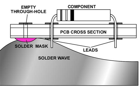
Inadequate solder mask design: If the solder mask opening around the pads is too large or if there is insufficient solder mask between adjacent pads, molten solder can easily flow beyond the intended area.
-
Excessive solder paste application: Applying too much solder paste on the pads can lead to solder overflow and wicking during reflow.
-
Improper reflow profile: An incorrect reflow temperature profile, such as a peak temperature that is too high or a soak time that is too long, can cause the solder to remain in a molten state for an extended period, increasing the likelihood of solder escape.
-
Component placement issues: Misaligned or improperly seated components can create gaps or uneven surfaces that promote solder wicking.
-
Surface contamination: Contaminants on the PCB surface, such as flux residue or oils, can alter the surface tension of the molten solder and encourage its flow away from the intended joint.
Impact of Solder Escape on PCB Assembly
Solder escape can have several detrimental effects on the quality and reliability of the assembled PCB:
-
Bridging: When solder flows between adjacent pads, it can create unintended electrical connections, leading to short circuits and functional failures.
-
Insufficient solder joints: If too much solder escapes from the intended joint, there may not be enough remaining to form a strong and reliable connection between the component and the pad.
-
Reduced mechanical strength: Solder escape can weaken the mechanical bond between the component and the PCB, making the assembly more susceptible to damage from vibration or mechanical stress.
-
Aesthetic issues: Solder wicking can result in an unsightly appearance of the assembled PCB, which may be unacceptable for certain applications or customers.
-
Rework and repair challenges: Rectifying solder escape issues often requires manual rework, which can be time-consuming, costly, and potentially damaging to the PCB and components.
Strategies for Preventing Solder Escape
To minimize the occurrence of solder escape during reflow soldering, several strategies can be employed:
1. Optimizing Solder Mask Design
Proper solder mask design is crucial for preventing solder escape. Consider the following guidelines:
-
Ensure that the solder mask opening around the pads is appropriately sized. The opening should be slightly larger than the pad to allow for proper solder wetting, but not so large that it encourages solder wicking.
-
Maintain sufficient solder mask spacing between adjacent pads. A minimum spacing of 0.1 mm to 0.15 mm is generally recommended, depending on the PCB design rules and manufacturing capabilities.
-
Use solder mask dams or barriers to prevent solder flow between closely spaced pads or along component leads.
2. Controlling Solder Paste Application
Precise control over solder paste application is essential to prevent solder escape:
-
Use stencils with appropriate aperture sizes and shapes to deposit the correct amount of solder paste on each pad. The stencil thickness and aperture design should be optimized based on the component footprint and desired solder volume.
-
Regularly inspect and maintain the stencil to ensure clean and unobstructed apertures. Clogged or damaged apertures can lead to inconsistent solder paste deposition.
-
Implement solder paste inspection (SPI) systems to verify the accuracy and consistency of solder paste deposits before reflow. SPI can detect issues such as insufficient or excessive solder paste, bridging, or misalignment.
3. Optimizing Reflow Profile
A well-designed reflow temperature profile is crucial for minimizing solder escape:
-
Follow the recommended reflow profile provided by the solder paste manufacturer or component suppliers. Each solder paste has specific requirements for peak temperature, soak time, and ramp rates.
-
Avoid excessive peak temperatures or prolonged soak times, which can cause the solder to remain molten for too long, increasing the risk of solder escape.
-
Use a multi-zone reflow oven with precise temperature control to ensure consistent heating across the PCB.
-
Monitor the reflow process using thermocouples or profiling systems to verify that the actual temperature profile matches the intended profile.
4. Ensuring Proper Component Placement
Accurate component placement is essential for preventing solder escape:
-
Use pick-and-place machines with high placement accuracy to ensure that components are properly aligned and seated on the pads.
-
Implement vision systems or other inspection methods to verify component placement before reflow.
-
Consider using self-centering components or those with leads that help maintain proper alignment during reflow.
5. Maintaining Surface Cleanliness
Keeping the PCB surface clean and free from contaminants can help prevent solder escape:
-
Ensure that the PCB fabrication process includes proper cleaning steps to remove any residual flux, oils, or other contaminants.
-
Handle PCBs and components with gloves to avoid introducing oils or moisture from skin contact.
-
Store PCBs and components in a controlled environment with appropriate humidity and temperature levels to prevent surface contamination.

Troubleshooting Solder Escape Issues
Despite implementing preventive measures, solder escape may still occur occasionally. When faced with solder escape issues, consider the following troubleshooting steps:
-
Visual inspection: Carefully examine the affected area using a magnifying lens or microscope to assess the extent of solder escape and identify any obvious causes, such as bridging or insufficient solder.
-
Rework and repair: If the solder escape is localized and not widespread, manual rework using a soldering iron and solder wick can often resolve the issue. Carefully remove the excess solder and reflow the joint if necessary.
-
Cleaning: If surface contamination is suspected, clean the affected area with isopropyl alcohol or a specialized PCB Cleaning solution to remove any residues that may be contributing to solder escape.
-
Process analysis: Review the solder paste application, component placement, and reflow processes to identify any deviations from the optimal parameters. Adjust the process settings or equipment as needed to prevent future occurrences.
-
Design review: If solder escape persists despite process optimizations, review the PCB design, particularly the solder mask layout and component footprints. Consider modifying the design to incorporate solder mask dams, increase pad spacing, or adjust pad sizes.

Real-World Examples and Case Studies
To better understand the impact of solder escape and the effectiveness of preventive measures, let’s explore some real-world examples and case studies.
Example 1: Smartphone PCB Assembly
A smartphone manufacturer encountered frequent solder escape issues during the assembly of their main PCB. The solder was wicking along the leads of fine-pitch components, causing bridging and short circuits. The manufacturer implemented the following solutions:
- Redesigned the solder mask to include dams between adjacent pads and reduced the solder mask opening size.
- Optimized the solder paste stencil aperture design to deposit the appropriate amount of paste on each pad.
- Adjusted the reflow profile to reduce the peak temperature and soak time.
As a result, the occurrence of solder escape decreased significantly, improving the yield and reliability of the assembLED PCBs.
Example 2: Automotive Electronic Control Unit (ECU)
An automotive supplier was experiencing solder escape issues on the ECU boards, particularly around the high-density connector pins. The solder was flowing along the pins and creating bridges, leading to functional failures. The supplier took the following actions:
- Modified the PCB design to increase the spacing between the connector pins and added solder mask barriers.
- Implemented a solder paste inspection system to verify the accuracy and consistency of solder paste deposits.
- Conducted thorough cleaning of the PCBs and connectors before assembly to remove any surface contaminants.
These measures effectively reduced the occurrence of solder escape, improving the reliability and performance of the ECUs.

Frequently Asked Questions (FAQ)
-
What is solder escape, and why is it a concern in PCB assembly?
Solder escape, also known as solder wicking, is the unintended flow of molten solder away from the desired joint and onto adjacent areas of the PCB or component leads. It is a concern because it can cause bridging, insufficient solder joints, and reduced reliability of the assembled PCB. -
What are the main causes of solder escape?
The main causes of solder escape include inadequate solder mask design, excessive solder paste application, improper reflow profile, component placement issues, and surface contamination. -
How can solder mask design help prevent solder escape?
Proper solder mask design, such as appropriate sizing of solder mask openings, sufficient spacing between pads, and the use of solder mask dams or barriers, can help contain the flow of molten solder and prevent it from wicking onto unintended areas. -
What role does the reflow profile play in preventing solder escape?
The reflow profile, which defines the temperature and duration of the soldering process, plays a crucial role in preventing solder escape. An optimized reflow profile with appropriate peak temperature, soak time, and ramp rates can help minimize the time the solder remains molten, reducing the likelihood of solder escape. -
How can surface contamination contribute to solder escape, and what can be done to mitigate it?
Surface contamination, such as flux residue or oils, can alter the surface tension of the molten solder and encourage its flow away from the intended joint. To mitigate this, proper cleaning of the PCB and components before assembly, handling with gloves, and storing in a controlled environment can help maintain surface cleanliness and reduce the risk of solder escape.
Conclusion
Solder escape is a common challenge in PCB assembly that can lead to various issues, such as bridging, insufficient solder joints, and reduced reliability. By understanding the causes and implementing preventive measures, manufacturers can effectively mitigate the occurrence of solder escape and improve the quality of their assembled PCBs.
Key strategies for preventing solder escape include optimizing solder mask design, controlling solder paste application, fine-tuning the reflow profile, ensuring proper component placement, and maintaining surface cleanliness. When solder escape issues do arise, troubleshooting techniques such as visual inspection, rework, cleaning, process analysis, and design review can help identify and resolve the problem.
By adopting best practices and continuously monitoring and improving the assembly process, manufacturers can minimize the impact of solder escape and produce high-quality, reliable PCBs that meet the demanding requirements of various industries.


Leave a Reply