Introduction to Bluetooth PCB Guidelines
Bluetooth technology has become ubiquitous in modern electronic devices, enabling seamless wireless communication between devices. As a result, the demand for well-designed Bluetooth circuit boards has increased significantly. Designing a Bluetooth PCB requires careful consideration of various factors to ensure optimal performance, reliability, and cost-effectiveness. In this article, we will discuss the best design guidelines for Bluetooth circuit boards, covering topics such as component selection, layout considerations, and testing procedures.
Understanding Bluetooth Technology
What is Bluetooth?
Bluetooth is a wireless communication standard that allows devices to exchange data over short distances using radio waves. It operates in the 2.4 GHz ISM (Industrial, Scientific, and Medical) frequency band and uses frequency-hopping spread spectrum (FHSS) technology to avoid interference with other devices using the same frequency range.
Bluetooth Versions and Features
Over the years, Bluetooth technology has evolved, offering improved features and capabilities with each new version. The following table summarizes the key features of different Bluetooth versions:
| Bluetooth Version | Release Year | Max Data Rate | Range | Key Features |
|---|---|---|---|---|
| 1.0 | 1999 | 1 Mbps | 10 m | Basic data transfer |
| 2.0 + EDR | 2004 | 3 Mbps | 10 m | Enhanced Data Rate (EDR) |
| 3.0 + HS | 2009 | 24 Mbps | 10 m | High Speed (HS) with Wi-Fi |
| 4.0 (BLE) | 2010 | 1 Mbps | 50-100 m | Bluetooth Low Energy (BLE) |
| 5.0 | 2016 | 2 Mbps | 240 m | Increased speed, range, and broadcast capacity |
| 5.1 | 2019 | 2 Mbps | 240 m | Direction finding and improved location accuracy |
| 5.2 | 2020 | 2 Mbps | 240 m | Enhanced Attribute Protocol (EATT) and power control |
Bluetooth Profiles and Use Cases
Bluetooth profiles define the capabilities and requirements for specific use cases. Some common Bluetooth profiles include:
- A2DP (Advanced Audio Distribution Profile): Streaming high-quality audio
- HFP (Hands-Free Profile): Hands-free communication in cars
- HID (Human Interface Device Profile): Connecting keyboards, mice, and game controllers
- SPP (Serial Port Profile): Emulating a serial port connection for data transfer

Bluetooth PCB Design Considerations
Component Selection
Choosing the right components is crucial for designing a reliable and cost-effective Bluetooth PCB. Consider the following factors when selecting components:
-
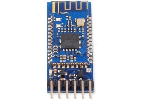
Bluetooth Module: Select a module that supports the desired Bluetooth version and profiles. Popular options include modules from manufacturers like Murata, Panasonic, and Laird.
-
Antenna: Choose an antenna that matches the frequency range and gain requirements of your application. Options include chip antennas, PCB trace antennas, and external antennas.
-
Power Management: Ensure that the power management components, such as voltage regulators and DC-DC converters, can efficiently supply the required power to the Bluetooth module and other components.
-
Crystals and Oscillators: Select high-quality, low-jitter crystals or oscillators to ensure accurate timing and minimize interference.
PCB Layout Guidelines
Proper PCB layout is essential for optimizing the performance and reliability of a Bluetooth circuit board. Follow these guidelines:
-
Ground Plane: Use a solid ground plane to minimize electromagnetic interference (EMI) and provide a low-impedance return path for high-frequency signals.
-
Power Supply Decoupling: Place decoupling capacitors close to the power pins of the Bluetooth module and other sensitive components to minimize power supply noise.
-
Antenna Placement: Position the antenna away from noisy components and ensure that it has a clear path for signal propagation. Follow the manufacturer’s guidelines for antenna placement and keep-out zones.
-
Signal Routing: Route high-speed signals, such as RF and clock lines, using controlled impedance traces. Avoid sharp bends and keep the traces as short as possible to minimize reflections and signal degradation.
-
Component Placement: Place components strategically to minimize signal path lengths and crosstalk. Keep noisy components, such as switching regulators, away from sensitive analog and RF circuits.
Electromagnetic Compatibility (EMC)
Ensuring electromagnetic compatibility is crucial for Bluetooth PCBs to avoid interference with other devices and comply with regulatory requirements. Consider the following EMC aspects:
-
Shielding: Use shielding techniques, such as metal cans or conformal shielding, to contain electromagnetic emissions from noisy components.
-
Filtering: Implement appropriate filtering techniques, such as ferrite beads and LC filters, to suppress high-frequency noise on power and signal lines.
-
Grounding: Ensure proper grounding of all components and shields to minimize ground loops and provide a low-impedance path for EMI currents.
-
Regulatory Compliance: Ensure that your Bluetooth PCB design complies with relevant EMC regulations, such as FCC Part 15 and CE, by conducting appropriate tests and obtaining certifications.

Bluetooth PCB Testing and Verification
Functional Testing
Perform functional tests to verify that the Bluetooth PCB operates as intended. This includes:
-
Connectivity Tests: Verify that the Bluetooth module can establish a connection with other devices and maintain a stable link.
-
Data Transfer Tests: Test data transfer functionality by sending and receiving data packets and verifying their integrity.
-
Range Tests: Conduct range tests to ensure that the Bluetooth PCB can maintain a connection at the desired distances.
RF Performance Testing
Evaluate the RF performance of the Bluetooth PCB to ensure optimal signal quality and minimize interference. This involves:
-
Spectrum Analysis: Use a spectrum analyzer to measure the frequency response, power levels, and spurious emissions of the Bluetooth PCB.
-
Antenna Performance: Measure antenna parameters such as gain, efficiency, and radiation patterns to verify that the antenna meets the design requirements.
-
Sensitivity and Selectivity: Test the receiver sensitivity and selectivity to ensure that the Bluetooth PCB can receive weak signals and reject interference from adjacent channels.
Reliability Testing
Conduct reliability tests to ensure that the Bluetooth PCB can withstand the intended operating conditions and have a long lifespan. This includes:
-
Environmental Testing: Expose the PCB to various environmental conditions, such as temperature, humidity, and vibration, to verify its robustness.
-
Accelerated Life Testing: Perform accelerated life tests to estimate the long-term reliability of the Bluetooth PCB under normal operating conditions.
-
Failure Analysis: Analyze any failures observed during testing to identify the root causes and implement corrective actions.

Frequently Asked Questions (FAQ)
-
What is the typical range of a Bluetooth connection?
The range of a Bluetooth connection depends on the Bluetooth version and the power class of the devices. Bluetooth 5.0 and later versions can achieve ranges up to 240 meters in open spaces, while earlier versions typically have a range of 10-100 meters. -
Can multiple Bluetooth devices be connected simultaneously?
Yes, Bluetooth allows multiple devices to be connected simultaneously. The exact number of devices that can be connected depends on the Bluetooth version and the device’s hardware and software capabilities. -
What is the difference between Bluetooth Classic and Bluetooth Low Energy (BLE)?
Bluetooth Classic is designed for continuous data streaming and has higher power consumption, while Bluetooth Low Energy is optimized for low power consumption and is ideal for applications that require infrequent data transfers, such as sensor data or device control. -
How can I ensure that my Bluetooth PCB is compliant with regulatory standards?
To ensure regulatory compliance, design your Bluetooth PCB following the guidelines provided by the Bluetooth SIG and the relevant regulatory bodies (e.g., FCC, CE). Conduct thorough testing and obtain necessary certifications before releasing the product to the market. -
What are some common challenges in designing Bluetooth PCBs?
Some common challenges in designing Bluetooth PCBs include minimizing electromagnetic interference, optimizing antenna performance, ensuring power efficiency, and achieving reliable connectivity. Careful component selection, proper PCB layout, and thorough testing can help overcome these challenges.
Conclusion
Designing a reliable and high-performance Bluetooth PCB requires careful consideration of various factors, including component selection, layout optimization, and electromagnetic compatibility. By following the guidelines discussed in this article and conducting thorough testing and verification, you can create a Bluetooth PCB that meets your application’s requirements and exceeds user expectations. As Bluetooth technology continues to evolve, staying up-to-date with the latest advancements and best practices will help you design future-proof Bluetooth PCBs that stand the test of time.


Leave a Reply