What is PCB Tenting?
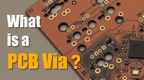
PCB Tenting, also known as Via Tenting or Tenting Vias, is a process used in the manufacturing of printed circuit boards (PCBs) where the vias (the small holes that allow electrical connections between layers of the PCB) are covered with a thin layer of solder mask material. This process is crucial in ensuring the reliability and functionality of the PCB.
The primary purpose of PCB Tenting is to protect the vias from contamination during the soldering process. Without tenting, solder can flow into the vias, causing short circuits and other issues that can compromise the integrity of the PCB. Tenting also helps to strengthen the mechanical structure of the PCB, making it more durable and resistant to damage.
Types of PCB Tenting
There are two main types of PCB Tenting:
-
Full Tenting: In this method, the entire via is covered with solder mask material, creating a completely sealed hole. This provides the highest level of protection against contamination and mechanical stress.
-
Partial Tenting: Also known as “Mask Defined” tenting, this method involves covering only the annular ring (the copper pad surrounding the via hole) with solder mask material. The hole itself remains open, allowing for better outgassing during the soldering process.
The choice between full and partial tenting depends on the specific requirements of the PCB design and the manufacturing process being used.
Importance of PCB Tenting
PCB Tenting plays a vital role in ensuring the quality, reliability, and longevity of printed circuit boards. Some of the key benefits of PCB Tenting include:
1. Protection against contamination
One of the primary advantages of PCB Tenting is its ability to protect vias from contamination during the soldering process. When a PCB undergoes soldering, there is a risk of solder flowing into the vias, which can cause short circuits and other issues. By covering the vias with a layer of solder mask material, PCB Tenting prevents solder from entering the holes, ensuring a clean and reliable connection between layers.
2. Improved mechanical strength
Tenting also helps to improve the mechanical strength of the PCB. The solder mask material used in tenting acts as a reinforcement for the vias, making them more resistant to mechanical stress and damage. This is particularly important for PCBs that will be subjected to high levels of vibration or physical strain, such as those used in automotive or aerospace applications.
3. Enhanced electrical insulation
Another benefit of PCB Tenting is its ability to enhance the electrical insulation of the vias. By covering the vias with a non-conductive solder mask material, tenting helps to prevent electrical leakage and crosstalk between adjacent vias. This is crucial for High-Frequency PCB Designs, where even small amounts of electrical interference can cause significant problems.
4. Better thermal management
PCB Tenting can also help to improve the thermal management of the PCB. By sealing the vias, tenting prevents hot air from escaping through the holes during the soldering process. This helps to maintain a more consistent temperature across the PCB, reducing the risk of thermal stress and damage to components.
5. Increased manufacturing efficiency
Finally, PCB Tenting can help to increase the efficiency of the manufacturing process. By eliminating the need for additional steps such as Via Plugging or filling, tenting allows for faster and more streamlined production of PCBs. This can help to reduce manufacturing costs and lead times, making it an attractive option for high-volume PCB production.

PCB Tenting Process
The PCB Tenting process typically involves the following steps:
-
Solder Mask Application: A layer of liquid photoimageable solder mask material is applied to the surface of the PCB using a screen printing or spraying method.
-
Exposure and Developing: The solder mask is then exposed to UV light through a photographic film or direct imaging process, which hardens the areas that will remain on the PCB. The unexposed areas are then removed using a developing solution.
-
Curing: The solder mask is cured using heat to fully harden and adhere to the PCB surface.
-
Inspection: The tented PCB is inspected for any defects or inconsistencies in the solder mask coverage.
The specific details of the PCB Tenting process may vary depending on the manufacturer and the type of solder mask material being used.

Factors Affecting PCB Tenting Quality
Several factors can impact the quality and effectiveness of PCB Tenting:
1. Via size and aspect ratio
The size and aspect ratio (depth to width ratio) of the vias can affect the ability of the solder mask material to fully cover and seal the holes. Smaller vias with higher aspect ratios may be more difficult to tent effectively.
2. Solder mask material properties
The type and quality of the solder mask material used can also impact the success of PCB Tenting. Factors such as viscosity, thermal stability, and adhesion strength can all affect the ability of the solder mask to fully cover and protect the vias.
3. Manufacturing process parameters
The specific parameters used in the PCB Tenting process, such as the screen printing or spraying method, exposure time, and curing temperature, can also affect the quality of the tenting. Careful optimization of these parameters is necessary to ensure consistent and reliable results.
4. PCB design and layout
The design and layout of the PCB can also impact the effectiveness of PCB Tenting. Factors such as the placement and spacing of vias, the presence of other components or features near the vias, and the overall complexity of the PCB design can all affect the ability to achieve high-quality tenting.

Best Practices for PCB Tenting
To ensure the best possible results from PCB Tenting, consider the following best practices:
-
Choose the right solder mask material: Select a solder mask material that is well-suited to the specific requirements of your PCB design and manufacturing process. Consider factors such as viscosity, thermal stability, and adhesion strength.
-
Optimize via size and placement: Where possible, design vias with a size and aspect ratio that is conducive to effective tenting. Avoid placing vias too close together or near other components that could interfere with the tenting process.
-
Control manufacturing process parameters: Carefully monitor and control the key parameters of the PCB Tenting process, such as screen printing or spraying method, exposure time, and curing temperature. Use statistical process control methods to ensure consistent results.
-
Perform regular inspections: Conduct regular inspections of tented PCBs to identify any defects or inconsistencies in the solder mask coverage. Use automated optical inspection (AOI) equipment where possible to ensure thorough and reliable inspections.
-
Work with experienced manufacturers: Partner with PCB manufacturers that have extensive experience and expertise in PCB Tenting. Look for manufacturers that use state-of-the-art equipment and processes and have a proven track record of producing high-quality tented PCBs.
Alternatives to PCB Tenting
While PCB Tenting is a widely used and effective method for protecting vias, there are some alternatives that may be suitable in certain situations:
1. Via plugging
Via plugging involves filling the vias with a non-conductive material, such as epoxy or resin, to seal them and prevent contamination. This method can provide a higher level of protection than tenting, but it is typically more expensive and time-consuming.
2. Via capping
Via capping involves placing a small, pre-formed cap over the via to seal it. This method can be faster and less expensive than via plugging, but it may not provide the same level of protection and durability as tenting.
3. Blind and buried vias
Blind and buried vias are types of vias that do not extend through the entire thickness of the PCB. Blind vias are exposed on only one side of the PCB, while buried vias are completely internal and not exposed on either side. These types of vias can help to reduce the need for tenting, but they may be more expensive and complex to manufacture.
FAQ
1. What is the difference between full and partial PCB Tenting?
Full PCB Tenting involves covering the entire via with solder mask material, while partial tenting (also known as “mask defined” tenting) involves covering only the annular ring around the via hole. Full tenting provides a higher level of protection, while partial tenting allows for better outgassing during soldering.
2. Can PCB Tenting be used on all types of PCBs?
PCB Tenting can be used on most types of PCBs, including rigid, flexible, and rigid-Flex Designs. However, the specific requirements and challenges of each type of PCB may require different approaches to tenting.
3. How does PCB Tenting affect the cost and lead time of PCB manufacturing?
PCB Tenting can help to reduce the cost and lead time of PCB manufacturing by eliminating the need for additional steps such as via plugging or filling. However, the specific impact on cost and lead time will depend on factors such as the complexity of the PCB design, the type of solder mask material used, and the manufacturing process parameters.
4. What are some common defects or issues that can occur with PCB Tenting?
Common defects or issues that can occur with PCB Tenting include incomplete or inconsistent coverage of the vias, bubbles or voids in the solder mask material, and peeling or delamination of the solder mask. These issues can be caused by factors such as improper manufacturing process parameters, contamination of the PCB surface, or incompatibility between the solder mask material and the PCB substrate.
5. How can I ensure the quality and reliability of PCB Tenting in my PCB designs?
To ensure the quality and reliability of PCB Tenting in your PCB designs, follow best practices such as choosing the right solder mask material, optimizing via size and placement, controlling manufacturing process parameters, performing regular inspections, and working with experienced PCB manufacturers. It may also be helpful to conduct thorough testing and qualification of tented PCBs to validate their performance and reliability in the intended application.
Conclusion
PCB Tenting is a critical process in the manufacturing of high-quality, reliable printed circuit boards. By protecting vias from contamination, improving mechanical strength, enhancing electrical insulation, and enabling better thermal management, PCB Tenting helps to ensure the overall performance and longevity of PCBs.
To achieve the best results from PCB Tenting, it is important to carefully consider factors such as via size and placement, solder mask material properties, manufacturing process parameters, and PCB design and layout. By following best practices and working with experienced PCB manufacturers, designers and engineers can leverage the benefits of PCB Tenting to create PCBs that meet the demands of even the most challenging applications.
As PCB technology continues to evolve, the role of PCB Tenting is likely to remain significant. By staying up-to-date with the latest developments and techniques in PCB Tenting, PCB designers and manufacturers can continue to push the boundaries of what is possible with printed circuit boards, enabling new and innovative electronic products and systems.


Leave a Reply