Introduction to SMT Stencils
Surface Mount Technology (SMT) has revolutionized the electronics manufacturing industry by enabling the production of smaller, faster, and more efficient electronic devices. One of the critical components in the SMT Assembly process is the solder paste stencil, also known as the SMT stencil. This article will delve into the world of SMT Stencils, exploring their importance, types, materials, design considerations, and best practices for achieving optimal results in Electronic Assembly.
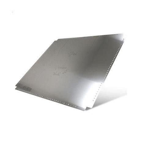
What is an SMT Stencil?
An SMT stencil is a thin metal sheet with precise openings that correspond to the pads on a printed circuit board (PCB). The stencil is used to apply solder paste onto the PCB pads before placing the electronic components. The solder paste deposited through the stencil openings ensures a uniform and accurate amount of solder is applied to each pad, resulting in reliable and consistent solder joints.
The Importance of SMT Stencils in Electronic Assembly
SMT stencils play a crucial role in the electronic assembly process for several reasons:
- Precision: Stencils ensure accurate and consistent solder paste deposition, which is essential for creating reliable solder joints.
- Efficiency: Using stencils allows for the rapid application of solder paste to multiple PCBs simultaneously, increasing production throughput.
- Miniaturization: As electronic devices become smaller and more compact, SMT stencils enable the precise application of solder paste to tiny pads and fine-pitch components.
- Cost-effectiveness: Stencils help minimize solder paste waste and reduce the likelihood of defects, leading to cost savings in the long run.
Types of SMT Stencils
There are several types of SMT stencils available, each with its own characteristics and applications.
Laser-Cut Stencils
Laser-cut stencils are created using a high-precision laser to cut the openings in the stencil material. This method allows for the creation of intricate designs and fine features, making laser-cut stencils suitable for high-density PCBs and fine-pitch components. Laser-cut stencils offer excellent dimensional accuracy and smooth aperture walls, which contribute to the consistent deposition of solder paste.
Electroformed Stencils
Electroformed stencils are manufactured using an electroplating process, where the stencil material is deposited onto a master pattern. This process enables the creation of stencils with highly precise and uniform apertures, even for very fine features. Electroformed stencils are known for their superior printing performance and long lifespan, making them ideal for high-volume production and applications requiring exceptional accuracy.
Chemically Etched Stencils
Chemically etched stencils are produced by selectively removing material from a metal sheet using a chemical etching process. This method is less precise compared to laser-cutting or electroforming, but it is more cost-effective for larger apertures and lower-density PCBs. Chemically etched stencils are suitable for applications with less stringent accuracy requirements and larger component sizes.
Additive Stencils
Additive stencils, also known as E-fab or electropolished additive stencils, are created by electroplating the stencil material onto a thin, temporary substrate. The substrate is then removed, leaving behind a free-standing stencil with smooth aperture walls and a uniform thickness. Additive stencils offer excellent printing performance and are well-suited for applications requiring fine-pitch components and high-density PCBs.

SMT Stencil Materials
The choice of material for an SMT stencil depends on several factors, including the desired lifespan, printing performance, and cost. The most common materials used for SMT stencils are:
Stainless Steel
Stainless steel is the most widely used material for SMT stencils due to its durability, stability, and cost-effectiveness. Stainless steel stencils offer excellent printing performance and can withstand multiple cleaning cycles, making them suitable for high-volume production. The most common stainless steel grades used for stencils are 304 and 316, with 316 being more resistant to corrosion.
Nickel
Nickel stencils are known for their exceptional durability and long lifespan, making them ideal for high-volume production runs. Nickel’s hardness and resistance to wear make it an excellent choice for applications requiring frequent stencil cleaning and handling. However, nickel stencils are more expensive compared to stainless steel and may not be as cost-effective for shorter production runs.
Polyimide
Polyimide stencils, also known as polymer stencils, are made from a flexible, non-metallic material. These stencils are lightweight, easy to handle, and resistant to stretching and tearing. Polyimide stencils are particularly useful for applications involving flexible circuits or low-volume prototyping. However, they may not be as durable as metal stencils and have limitations in terms of minimum feature sizes.

SMT Stencil Design Considerations
Designing an effective SMT stencil involves several key considerations to ensure optimal solder paste deposition and printing performance.
Aperture Size and Shape
The size and shape of the stencil apertures directly impact the volume and distribution of solder paste deposited onto the PCB pads. Aperture dimensions should be carefully calculated based on the pad size, component pitch, and solder paste properties. Common aperture shapes include square, rectangular, and circular, with the choice depending on the specific component and pad geometry.
Stencil Thickness
Stencil thickness plays a crucial role in determining the volume of solder paste deposited and the printing process’s repeatability. Thicker stencils deposit more solder paste, which may be necessary for larger components or pads. However, thicker stencils can also lead to issues such as paste bridging and difficulty in releasing the stencil from the PCB. Thinner stencils, on the other hand, provide better print definition and are suited for finer-pitch components but may not deposit sufficient solder paste for larger pads.
| Stencil Thickness | Typical Application |
|---|---|
| 0.100 mm (4 mil) | Very fine-pitch components (0.3 mm pitch or less) |
| 0.125 mm (5 mil) | Fine-pitch components (0.4 mm to 0.5 mm pitch) |
| 0.150 mm (6 mil) | Standard SMD components (0.5 mm to 0.8 mm pitch) |
| 0.200 mm (8 mil) | Larger SMD components and connectors |
Aperture Wall Angle
The angle of the aperture walls in an SMT stencil affects the release of solder paste during the printing process. Aperture walls with a slightly tapered angle (typically 5° to 7°) facilitate the smooth release of solder paste and minimize the occurrence of paste hanging or sticking to the stencil. A well-designed aperture wall angle ensures clean and consistent solder paste deposits.
Fiducial Marks and Alignment Features
Fiducial marks and alignment features on the SMT stencil are essential for ensuring proper alignment between the stencil and the PCB during the printing process. These features, typically in the form of crosshairs or circles, are used by automated stencil printers to accurately position the stencil relative to the PCB. Proper alignment is critical for achieving precise solder paste deposition and preventing component misalignment during placement.

Best Practices for SMT Stencil Printing
To achieve optimal results in SMT stencil printing, consider the following best practices:
- Stencil Cleaning: Regularly clean the stencil to remove solder paste residue and prevent aperture clogging. Use appropriate cleaning agents and methods, such as manual cleaning with solvents or automated underside cleaning systems.
- Printer Setup: Ensure proper setup of the stencil printer, including alignment, pressure, and speed settings. Conduct regular calibration and maintenance to maintain optimal performance.
- Solder Paste Selection: Choose a solder paste with the appropriate particle size, flux activity, and rheological properties for your specific application and stencil design.
- Print Parameters: Optimize print parameters, such as squeegee pressure, speed, and separation distance, to achieve consistent solder paste deposits and minimize defects.
- Environmental Control: Maintain a controlled environment with stable temperature and humidity levels to ensure consistent solder paste behavior and prevent issues like paste drying or slumping.
Frequently Asked Questions (FAQ)
-
What is the difference between a solder paste stencil and a solder mask?
A solder paste stencil is a separate, thin metal sheet with openings used to apply solder paste onto PCB pads, while a solder mask is a permanent layer applied to the PCB itself to protect against solder bridging and define the solderable areas. -
How often should I clean my SMT stencil?
The frequency of stencil cleaning depends on factors such as the solder paste type, print volume, and environment. As a general guideline, clean the stencil every 4-8 hours of continuous printing or whenever print quality begins to deteriorate. -
Can I reuse an SMT stencil for different PCB designs?
While it is possible to reuse an SMT stencil for different PCB designs with similar pad layouts, it is generally recommended to use a dedicated stencil for each unique design to ensure optimal print quality and avoid potential issues related to aperture size and placement. -
What is the typical lifespan of an SMT stencil?
The lifespan of an SMT stencil depends on factors such as the stencil material, printing volume, and handling practices. A well-maintained stainless steel stencil can last for tens of thousands of prints, while a nickel stencil may last even longer. However, stencils should be regularly inspected for wear and replaced when print quality deteriorates. -
How do I store my SMT stencils when not in use?
Store SMT stencils in a clean, dry environment, away from direct sunlight and sources of heat or humidity. Use protective covers or containers to prevent damage and contamination. Avoid stacking stencils directly on top of each other to minimize the risk of scratches or deformation.
Conclusion
SMT stencils are a critical component in the electronic assembly process, enabling the precise and efficient application of solder paste onto PCB pads. By understanding the types, materials, design considerations, and best practices associated with SMT stencils, manufacturers can optimize their solder paste printing process and achieve high-quality, reliable solder joints.
As the electronics industry continues to evolve, with ever-increasing demands for miniaturization and performance, the role of SMT stencils in enabling these advancements cannot be overstated. By staying informed about the latest developments in stencil technology and adopting best practices in stencil design and maintenance, manufacturers can remain competitive and deliver cutting-edge electronic products to market.


Leave a Reply