Introduction to PCB Manufacturing
Printed Circuit Boards (PCBs) are the backbone of modern electronics. They provide a platform for interconnecting electronic components and form the foundation of devices ranging from simple consumer gadgets to complex aerospace systems. PCB manufacturing is a multi-step process that involves design, fabrication, assembly, and testing. In this comprehensive article, we will delve into the intricacies of PCB manufacturing and explore ways to optimize the process for better results.
Understanding the PCB Manufacturing Process
Step 1: PCB Design
The PCB manufacturing process begins with the design phase. Engineers use specialized software to create a schematic diagram and a layout of the PCB. The schematic represents the electrical connections between components, while the layout determines the physical placement of components and routing of traces on the board.
Key Considerations in PCB Design
- Component selection and placement
- Signal integrity and electromagnetic compatibility
- Thermal management
- Manufacturing constraints and design for manufacturability (DFM)
Step 2: PCB Fabrication
Once the design is finalized, the PCB fabrication process begins. This involves creating a physical board based on the digital design files. The fabrication process consists of several sub-steps:
PCB Fabrication Sub-Steps
-
Substrate Preparation: A substrate material, typically FR-4 (a glass-reinforced epoxy laminate), is cut to the desired size and shape.
-
Copper Cladding: The substrate is laminated with a thin layer of copper on one or both sides, depending on the design requirements.
-
Drilling: Holes are drilled through the board to accommodate through-hole components and create vias for inter-layer connections.
-
Patterning: The copper layer is selectively removed to create the desired circuit pattern. This is typically done using a photolithography process involving the application of a photoresist, exposure to UV light, and etching.
-
Plating: The board undergoes various plating processes, such as electroless copper plating, to ensure proper electrical connectivity and protect the exposed copper traces.
-
Solder Mask Application: A protective solder mask is applied to the board, leaving only the areas intended for soldering exposed.
-
Silkscreen Printing: Text, symbols, and logos are printed on the board using a silkscreen process for identification and assembly guidance.
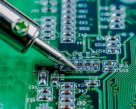
Step 3: PCB Assembly
After the bare PCB is fabricated, it undergoes the assembly process to populate it with electronic components. The assembly process can be divided into two main categories: through-hole assembly and surface mount assembly.
Through-Hole Assembly (THA)
In through-hole assembly, components with long leads are inserted into drilled holes on the PCB and soldered in place. This method is suitable for larger components and provides strong mechanical connections.
Surface Mount Assembly (SMT)
Surface mount assembly involves placing components directly onto the surface of the PCB and soldering them in place. SMT allows for smaller component sizes, higher component density, and faster assembly compared to THA.
Step 4: PCB Testing and Inspection
To ensure the quality and functionality of the assembled PCB, various testing and inspection procedures are carried out. These include:
- Visual inspection
- Automated Optical Inspection (AOI)
- X-ray inspection
- In-Circuit Testing (ICT)
- Functional testing

Optimizing PCB Manufacturing for Better Results
Design for Manufacturability (DFM)
One of the key aspects of improving PCB manufacturing is incorporating DFM principles into the design process. DFM involves designing the PCB in a way that facilitates efficient and reliable manufacturing. Some DFM guidelines include:
- Adhering to minimum trace width and spacing requirements
- Avoiding sharp angles in traces
- Providing adequate clearance around components
- Using standard component sizes and footprints
- Minimizing the number of unique components
| DFM Guideline | Benefit |
|---|---|
| Adhere to minimum trace width and spacing | Ensures reliable manufacturing and reduces defects |
| Avoid sharp angles in traces | Improves signal integrity and reduces manufacturing issues |
| Provide adequate clearance around components | Facilitates proper soldering and reduces assembly defects |
| Use standard component sizes and footprints | Simplifies sourcing and reduces inventory costs |
| Minimize the number of unique components | Streamlines assembly and reduces the risk of errors |
Material Selection
Choosing the right materials for PCB manufacturing is crucial for achieving the desired performance and reliability. Factors to consider when selecting materials include:
- Dielectric constant and loss tangent of the substrate material
- Thermal conductivity and coefficient of thermal expansion (CTE)
- Copper weight and thickness
- Solder mask and silkscreen ink properties
| Material Property | Impact on PCB Performance |
|---|---|
| Dielectric constant and loss tangent | Affects signal integrity and high-frequency performance |
| Thermal conductivity and CTE | Influences heat dissipation and thermal stress management |
| Copper weight and thickness | Determines current carrying capacity and signal integrity |
| Solder mask and silkscreen ink properties | Affects solderability, protection, and legibility |
Process Control and Quality Management
Implementing robust process control and quality management systems is essential for consistently producing high-quality PCBs. Some key aspects of process control and quality management include:
- Establishing and maintaining process parameters within specified limits
- Implementing statistical process control (SPC) techniques
- Conducting regular calibration and maintenance of manufacturing equipment
- Performing incoming material inspections and supplier quality management
- Implementing traceability and lot tracking systems
| Process Control Technique | Benefit |
|---|---|
| Establishing and maintaining process parameters | Ensures consistent output and reduces process variability |
| Implementing SPC techniques | Identifies and corrects process deviations early |
| Regular calibration and maintenance | Maintains equipment accuracy and prevents defects |
| Incoming material inspections | Catches quality issues before they enter production |
| Traceability and lot tracking | Enables quick identification and containment of issues |
Continuous Improvement and Lean Manufacturing
Embracing a culture of continuous improvement and implementing lean manufacturing principles can significantly enhance PCB Manufacturing Efficiency and quality. Some strategies for continuous improvement and lean manufacturing include:
- Conducting regular Kaizen events to identify and eliminate waste
- Implementing 5S methodology for workplace organization and standardization
- Utilizing value stream mapping to optimize process flow
- Applying Just-In-Time (JIT) principles for inventory management
- Encouraging employee involvement and cross-functional collaboration
| Lean Manufacturing Technique | Benefit |
|---|---|
| Kaizen events | Fosters a culture of continuous improvement |
| 5S methodology | Improves workplace efficiency and reduces errors |
| Value stream mapping | Identifies and eliminates non-value-added activities |
| Just-In-Time (JIT) principles | Reduces inventory costs and improves material flow |
| Employee involvement and collaboration | Leverages the knowledge and skills of the entire team |

Frequently Asked Questions (FAQ)
-
What is the difference between through-hole and surface mount assembly?
Through-hole assembly involves inserting component leads into drilled holes and soldering them in place, while surface mount assembly places components directly onto the surface of the PCB and solders them in place. Surface mount assembly allows for smaller component sizes and higher component density compared to through-hole assembly. -
What is Design for Manufacturability (DFM) and why is it important?
Design for Manufacturability (DFM) is the practice of designing PCBs in a way that facilitates efficient and reliable manufacturing. DFM principles include adhering to minimum trace width and spacing requirements, avoiding sharp angles in traces, providing adequate clearance around components, using standard component sizes and footprints, and minimizing the number of unique components. Incorporating DFM guidelines into the design process helps reduce manufacturing defects, improves yields, and lowers production costs. -
What are some key material properties to consider when selecting PCB materials?
When selecting PCB materials, it is essential to consider properties such as the dielectric constant and loss tangent of the substrate material, thermal conductivity and coefficient of thermal expansion (CTE), copper weight and thickness, and solder mask and silkscreen ink properties. These properties influence signal integrity, high-frequency performance, heat dissipation, thermal stress management, current carrying capacity, solderability, protection, and legibility of the PCB. -
How can process control and quality management improve PCB manufacturing?
Implementing robust process control and quality management systems helps ensure consistent production of high-quality PCBs. Key aspects include establishing and maintaining process parameters within specified limits, implementing statistical process control (SPC) techniques, conducting regular calibration and maintenance of manufacturing equipment, performing incoming material inspections and supplier quality management, and implementing traceability and lot tracking systems. These measures help identify and correct process deviations early, maintain equipment accuracy, catch quality issues before they enter production, and enable quick identification and containment of issues. -
What are some strategies for continuous improvement and lean manufacturing in PCB production?
Embracing a culture of continuous improvement and implementing lean manufacturing principles can significantly enhance PCB manufacturing efficiency and quality. Strategies include conducting regular Kaizen events to identify and eliminate waste, implementing 5S methodology for workplace organization and standardization, utilizing value stream mapping to optimize process flow, applying Just-In-Time (JIT) principles for inventory management, and encouraging employee involvement and cross-functional collaboration. These techniques foster a culture of continuous improvement, improve workplace efficiency, reduce errors, eliminate non-value-added activities, reduce inventory costs, improve material flow, and leverage the knowledge and skills of the entire team.

Conclusion
PCB manufacturing is a complex process that requires careful design, material selection, process control, and continuous improvement to achieve optimal results. By understanding the intricacies of the manufacturing process, incorporating DFM principles, selecting the right materials, implementing robust process control and quality management systems, and embracing lean manufacturing principles, PCB manufacturers can consistently produce high-quality boards that meet the ever-increasing demands of modern electronics.
As technology continues to advance and the complexity of PCBs grows, it is essential for manufacturers to stay updated with the latest industry trends, best practices, and innovative solutions. By investing in continuous learning, collaborating with suppliers and customers, and fostering a culture of excellence, PCB manufacturers can position themselves for long-term success in this dynamic and challenging industry.


Leave a Reply