Introduction to PLCC Packages
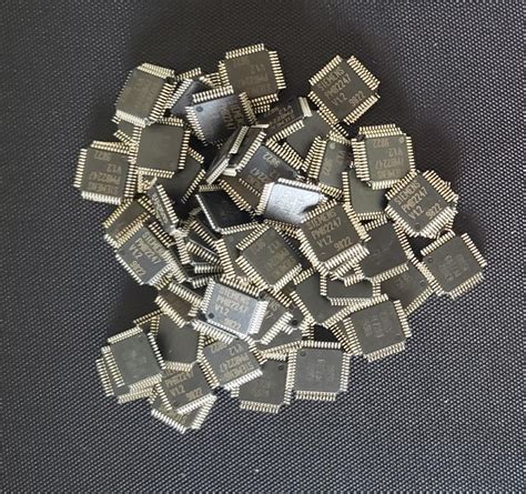
PLCC, which stands for Plastic Leaded Chip Carrier, is a type of surface-mount integrated circuit package used for housing and protecting electronic components. PLCC packages provide a compact, cost-effective solution for mounting ICs onto printed circuit boards (PCBs).
Key Characteristics of PLCC Packages
PLCC packages have several distinguishing features:
- Rectangular or square plastic housing
- J-shaped metal leads extending from all four sides
- Leads are designed to be soldered directly onto PCB Pads
- Provides good thermal and electrical performance
- Available in various sizes (20-84 pins) to accommodate different IC designs
The J-leads allow PLCC packages to be mounted either in socket adapters or soldered directly to the PCB surface. This versatility, along with their compact size and good performance, has made PLCCs a popular SMT package choice for many years.
PLCC Package Construction and Materials
Package Housing
PLCC packages use a molded plastic housing to encapsulate and protect the internal silicon die and wire bonds. The housing is typically made of a durable epoxy resin that can withstand the high temperatures of the soldering process.
The package housing has a central cavity where the IC die is mounted. A metal leadframe is encased within the molded plastic. The leadframe is stamped or etched from a thin metal sheet, usually an alloy of copper or iron-nickel. The J-leads that extend from the package are part of this leadframe.
Die Attachment and Wire Bonding
Inside the cavity, the silicon IC die is attached to the leadframe using either a conductive epoxy or Eutectic Solder. This die attach provides both mechanical support and an electrical and thermal path to dissipate heat from the die to the leadframe.
After die attach, tiny gold or aluminum wires are bonded between the die bonding pads and the inner tips of the leadframe fingers. Wire bonding is a delicate process that uses either thermosonic or ultrasonic energy to weld the wires in place. The wire bonds create the electrical connections between the IC and package leads.
Molding and Marking
With the die and wire bonds in place, the package is transfer molded with the epoxy resin to form its final shape. Molding occurs under high pressure and temperature to ensure the epoxy fully encapsulates the die and bonds to the leadframe.
After molding, most PLCC packages undergo a laser marking process to cut the desired product information onto the surface of the plastic. Key details marked on the package include the manufacturer’s logo, part number, pin-1 indicator, and lot traceability codes.

PLCC Package Variations and Sizes
PLCC packages come in a range of standard sizes with different pin counts to suit the requirements of various IC devices. Here are some of the most common PLCC package sizes and their key dimensions:
| PLCC Size | Pin Count | Body Size (mm) | Lead Pitch (mm) |
|---|---|---|---|
| PLCC-20 | 20 | 8.9 x 9.7 | 1.27 |
| PLCC-28 | 28 | 11.5 x 11.5 | 1.27 |
| PLCC-32 | 32 | 11.5 x 14.0 | 1.27 |
| PLCC-44 | 44 | 16.6 x 16.6 | 1.27 |
| PLCC-52 | 52 | 18.9 x 18.9 | 1.27 |
| PLCC-68 | 68 | 24.1 x 24.1 | 1.27 |
| PLCC-84 | 84 | 30.2 x 30.2 | 1.27 |
The lead pitch, or distance between lead centers, is standardized at 1.27mm for all common PLCC packages. This allows the use of common PCB footprints and socket designs.
Some less common PLCC package sizes include the PLCC-22 (5.3 x 10.2mm), PLCC-62 (22.2 x 22.2mm), and PLCC-80 (26.1 x 26.1mm). These are generally only used for specialized applications.

PCB Design Considerations for PLCC Packages
When designing a PCB to accept a PLCC package, there are several key factors to consider to ensure proper fit, solderability, and reliability.
PCB Footprint and Land Pattern
The PCB footprint for a PLCC package consists of a set of copper pads that match the arrangement and pitch of the package’s J-leads. The pads must be the correct size and shape to allow for proper soldering and joint formation.
The PLCC land pattern will have a square or rectangular ring of pads with additional space in the center to accommodate the package body. The pad size and spacing are determined by the package dimensions and industry standards for SMT Soldering.
Some common PLCC package PCB land patterns are:
| PLCC Size | Pad Width (mm) | Pad Length (mm) | Pad Pitch (mm) |
|---|---|---|---|
| PLCC-20 | 0.6 | 2.2 | 1.27 |
| PLCC-28 | 0.6 | 2.2 | 1.27 |
| PLCC-44 | 0.6 | 2.2 | 1.27 |
| PLCC-84 | 0.7 | 2.8 | 1.27 |
It’s important to follow the recommended land pattern dimensions closely to avoid soldering defects like opens, shorts, or poor wetting.
Thermal Relief and Solder Mask
For PLCC packages with higher pin counts and power dissipation, it’s often necessary to include thermal relief pads or vias on the PCB footprint. Thermal reliefs are added copper areas or vias that help conduct heat away from the package leads into the board’s internal ground or power planes.
Proper design of thermal relief can help prevent overheating of the package and PCB during soldering and improve joint reliability. The size and spacing of thermal vias depends on the package power and PCB layout.
Solder mask is also an important consideration in the PLCC footprint design. Solder mask is a polymer coating applied to the PCB that prevents solder from bridging between adjacent pads. Solder mask openings should be sized to match the copper pads with a small buffer to account for alignment tolerances.
Placement and Routing
Proper placement and routing are critical for PLCC packages to avoid signal integrity and EMI issues. The package should be placed to minimize the length of critical signal traces and provide clean routes for power and ground.
Bypass Capacitors should be placed as close to the package power pins as possible to reduce noise. A ground plane layer should be used underneath the package to provide a low-impedance return path for high-speed signals.
Trace widths and spacings must be carefully designed to maintain characteristic impedance and avoid crosstalk. Differential pair traces should be length-matched and routed closely together.
Following good PCB layout practices and using simulation tools to validate the design can help ensure optimal performance and reliability of PLCCs in the final application.

PLCC Soldering Process and Guidelines
Soldering PLCC packages onto a PCB requires careful process control and technique to achieve reliable, defect-free solder joints. The basic steps in PLCC soldering are:
-
Solder Paste Application: A precise volume of solder paste is applied to the PCB PADS using a stencil or dispensing system. The paste volume must be consistent and sufficient to form a good joint.
-
Package Placement: The PLCC package is placed onto the PCB with its leads aligned to the pasted pads. Placement accuracy is critical to ensure the leads make good contact with the paste.
-
Reflow Soldering: The assembly is heated in a reflow oven following a precise temperature profile. The solder paste melts and wets the package leads and PCB pads, forming a metallurgical bond as it cools.
-
Inspection and Rework: After reflow, the solder joints are inspected visually or with X-ray to check for defects like opens, shorts, or voids. Any defective joints must be reworked using a soldering iron or rework station.
To achieve optimal results, the reflow profile must be tuned to the specific PLCC package size, thermal mass, and solder paste composition. Key profile parameters include:
- Preheat Ramp Rate: 1-3°C/sec
- Preheat Temperature: 150-180°C
- Soak Time: 60-120 sec
- Peak Temperature: 235-250°C
- Time Above Liquidus: 60-90 sec
- Cooling Rate: 1-6°C/sec
Proper control of the peak temperature and time above liquidus is essential to avoid thermal damage to the package and PCB while ensuring good wetting and joint formation.
The choice of solder paste alloy and flux chemistry is also important for PLCC soldering. Lead-free alloys like SAC305 are commonly used to meet RoHS requirements. The flux must provide good wetting and activiity without leaving corrosive residues.
Cleaning may be required after soldering to remove any remaining flux residues, especially for no-clean fluxes. Cleaning can be done with solvents or aqueous solutions depending on the flux type and PCB design.
By following good soldering practices and process controls, high-quality and reliable solder joints can be achieved with PLCC packages.
PLCC Socket Adapters and Applications
In some applications, it may be desirable to use a socket adapter instead of directly soldering the PLCC package to the PCB. Sockets provide several advantages:
- Allows for easy replacement or upgrade of the IC without soldering
- Reduces thermal and mechanical stress on the PCB during assembly
- Enables prototype debugging and testing of different ICs
PLCC sockets are available in various sizes to match the standard package dimensions. The socket consists of a plastic housing with metal contacts that mate with the PLCC leads. The socket is soldered to the PCB using through-hole or surface-mount terminations.
Some common types of PLCC sockets include:
- Through-hole (DIP) sockets
- Surface-mount (SMT) sockets
- Zero-insertion force (ZIF) sockets
- Burn-in and test sockets
Through-hole sockets are the simplest and lowest cost but require drilled holes in the PCB. SMT sockets are soldered to pads on the PCB surface, allowing for higher density and easier assembly. ZIF sockets use a lever or latch mechanism to allow the PLCC to be inserted or removed with minimal force, reducing wear on the leads.
Burn-in and test sockets are specialized adapters used for reliability testing and device programming. These sockets are designed for high insertion cycles and often have built-in temperature and signal monitoring capabilities.
When selecting a PLCC socket, key considerations include:
- Compatibility with the package size and pinout
- Contact material and plating for good electrical and mechanical performance
- Insertion force and cycle life
- Thermal and electrical specifications
- PCB footprint and layout requirements
Using a high-quality socket from a reputable supplier and following the manufacturer’s application guidelines can ensure reliable operation of the PLCC in the end system.
Common Applications of PLCC Packages
PLCC packages are used in a wide range of electronic applications across various industries. Some common uses of PLCCs include:
- Microcontrollers and processors
- Memory devices (EEPROM, SRAM, flash)
- Logic and interface ICs
- Analog and mixed-signal devices
- ASICs and FPGAs
- Telecommunications and networking equipment
- Industrial control and automation systems
- Consumer electronics and appliances
- Automotive and transportation electronics
- Medical devices and instrumentation
PLCCs are well-suited for these applications due to their good electrical and thermal performance, compact size, and versatility. The ability to use socket adapters also makes PLCCs a good choice for applications requiring field upgradeability or maintenance.
As technology advances, newer package styles like QFP and BGA have begun to replace PLCCs in some high-density applications. However, PLCCs remain a cost-effective and reliable choice for many designs, particularly in legacy and industrial systems.
PLCC Package Handling and Storage Guidelines
Proper handling and storage of PLCC packages is important to avoid damage and ensure optimal performance in the final application. Key guidelines include:
-
ESD Protection: PLCCs are sensitive to electrostatic discharge (ESD) and must be handled using proper grounding and static control measures. Personnel should wear grounded wrist straps and work on ESD-safe mats. Packages should be stored in conductive carriers or bags.
-
Moisture Sensitivity: PLCCs are moisture-sensitive devices (MSDs) and can absorb water from the air, leading to package cracking or delamination during reflow soldering. Packages should be stored in moisture-barrier bags with desiccant and humidity indicators. Exposure time out of the bag should be limited based on the package’s moisture sensitivity level (MSL) rating.
-
Temperature Control: Extreme temperatures can affect the package materials and lead to warpage or damage. PLCCs should be stored in a controlled environment with temperatures between 10-30°C and relative humidity below 60%.
-
Physical Handling: Rough handling or excessive force on the package leads can cause bending, breaking, or misalignment. Packages should be handled gently using vacuum pencils or tweezers. Leads should not be used as handles to pick up the package.
-
Solderability Maintenance: Oxidation or contamination of the package leads can affect solderability and joint reliability. Packages should be stored in sealed containers with sulfur-absorbing paper or desiccant to prevent oxidation. If leads become oxidized, they may need to be re-tinned before soldering.
By following these handling and storage guidelines, the risk of package damage and defects can be minimized, ensuring optimal performance and reliability in the final application.
Frequently Asked Questions (FAQ)
1. What does PLCC stand for?
PLCC stands for Plastic Leaded Chip Carrier. It is a type of surface-mount integrated circuit package with a rectangular plastic housing and J-shaped leads extending from all four sides.
2. What are the advantages of using PLCC packages?
PLCC packages offer several advantages, including:
– Compact size and high pin density
– Good electrical and thermal performance
– Versatility in mounting (can be soldered directly or used with socket adapters)
– Cost-effective for many applications
– Wide availability and standardization
3. How do I select the right PLCC package for my application?
When selecting a PLCC package, consider the following factors:
– Number of pins required for your device
– Electrical and thermal requirements (power dissipation, signal speed, etc.)
– PCB layout and space constraints
– Soldering process and equipment capabilities
– Cost and availability of the package and any required adapters
Consult with your IC vendor or packaging supplier to determine the best PLCC option for your specific needs.
4. Can PLCC packages be soldered by hand?
While it is possible to solder PLCC packages by hand using a soldering iron, it can be challenging due to the fine pitch and high number of leads. Hand soldering is not recommended for production assembly, as it is prone to defects and inconsistencies.
For prototyping or rework, a good technique is to use a fine-tipped iron with a temperature-controlled station and a microscope or magnifier to inspect the joints. Proper flux and solder wire gauge are also important for good results.
5. Are PLCC packages still used in new designs?
While PLCC packages have been largely replaced by newer styles like QFP and BGA in many high-density applications, they are still used in some new designs, particularly in industrial, automotive, and legacy systems.
PLCCs remain a cost-effective and reliable choice for applications that do not require the highest pin counts or performance. They are also still widely used for compatibility with existing socket adapters and PCB designs.
As technology continues to evolve, it is likely that PLCC usage will gradually decline in favor of more advanced package options. However, the large installed base and proven reliability of PLCCs ensure that they will continue to be used for many years to come.
Conclusion
PLCC packages have been a workhorse of the electronics industry for decades, providing a compact, reliable, and cost-effective solution for a wide range of applications. By understanding the key characteristics, variations, and design considerations of PLCCs, engineers and technicians can ensure optimal performance and reliability in their products.
Proper PCB layout, soldering process control, and handling and storage practices are essential for success with PLCC packages. The ability to use socket adapters also provides valuable flexibility for testing, prototyping, and field maintenance.
While newer package technologies continue to emerge, PLCCs remain a viable and trusted choice for many applications, particularly in legacy and industrial systems. By staying informed on best practices and industry trends, designers can make informed decisions on when and how to use PLCC packages


Leave a Reply