What is a PCB Stencil?
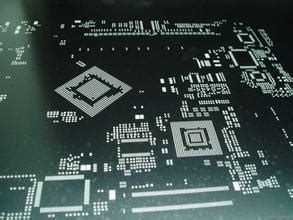
A PCB (printed circuit board) stencil, also known as a solder paste stencil, is a thin sheet of stainless steel or other material with laser-cut openings that correspond to the pads on a PCB. The stencil is used to apply solder paste onto the PCB pads before components are placed and the board goes through the reflow soldering process.
PCB stencils play a crucial role in the surface mount technology (SMT) assembly process by ensuring accurate and consistent solder paste application. This leads to better solder joints, fewer defects, and higher quality PCB assemblies.
Why Use a PCB Stencil?
There are several reasons why PCB stencils are essential in the SMT assembly process:
- Accuracy: PCB stencils ensure precise solder paste application on the pads, minimizing the risk of bridging, solder balls, or insufficient solder.
- Consistency: Using a stencil guarantees a uniform solder paste deposit across the entire PCB, leading to more consistent solder joints.
- Efficiency: Stencil printing is a fast and efficient method of applying solder paste, making it suitable for high-volume production.
- Cost-effective: Proper solder paste application using a stencil reduces the need for rework and touch-ups, saving time and money in the long run.

Types of PCB Stencils
There are two main types of PCB stencils:
-
Stainless Steel Stencils: These are the most common type of PCB stencils. They are durable, long-lasting, and suitable for high-volume production. Stainless steel stencils can be cleaned and reused multiple times.
-
Polyimide Stencils: Also known as polymer or plastic stencils, these are made from a flexible material that conforms to uneven PCB surfaces. Polyimide stencils are ideal for prototyping or low-volume production, as they are less expensive than stainless steel stencils but have a shorter lifespan.

Factors to Consider When Choosing a PCB Stencil Manufacturer
When selecting a PCB stencil manufacturer, there are several key factors to consider:
-
Quality: Look for a manufacturer that maintains high standards in terms of stencil accuracy, cleanliness, and durability. A good manufacturer will use state-of-the-art laser cutting equipment and follow strict quality control procedures.
-
Experience: Choose a manufacturer with a proven track record in the industry. Experienced manufacturers are more likely to have the knowledge and expertise to produce high-quality stencils and handle complex designs.
-
Turnaround Time: Consider the manufacturer’s lead times and ability to meet your deadlines. Some manufacturers offer expedited services for urgent projects.
-
Customer Support: Select a manufacturer that provides excellent customer support, including responsive communication, technical assistance, and after-sales service.
-
Price: While price is an important consideration, it shouldn’t be the sole deciding factor. Strike a balance between cost and quality to ensure you receive a high-quality stencil that meets your needs.

Top PCB Stencil Manufacturers
Here are some of the top PCB stencil manufacturers in the industry:
-
OSH Stencils: OSH Stencils is a leading provider of high-quality PCB stencils, offering both stainless steel and polyimide options. They are known for their fast turnaround times and excellent customer service.
-
Stencils Unlimited: With over 30 years of experience, Stencils Unlimited is a trusted source for PCB stencils. They offer a wide range of stencil types and thicknesses, as well as custom designs.
-
Pololu: Pololu is a well-known manufacturer of robotics and electronics components, including PCB stencils. They offer affordable, high-quality stainless steel stencils with quick turnaround times.
-
PCB Cart: PCB Cart is a full-service PCB manufacturer that also offers PCB stencil fabrication. They provide stainless steel stencils with a variety of thicknesses and aperture sizes.
-
PCBWay: PCBWay is a global PCB manufacturer that offers PCB stencil services. They provide both stainless steel and polyimide stencils, as well as custom designs and quick turnaround times.
PCB Stencil Design Guidelines
To ensure optimal solder paste application and high-quality PCB assemblies, follow these PCB stencil design guidelines:
-
Aperture Size: The aperture size should be slightly larger than the pad size to allow for proper solder paste release. A general rule of thumb is to add 10-20% to the pad size.
-
Aperture Shape: The aperture shape should match the pad shape as closely as possible. For example, use round apertures for round pads and square apertures for square pads.
-
Stencil Thickness: Choose the appropriate stencil thickness based on the solder paste particle size and the desired solder paste volume. A common thickness for standard SMT components is 0.1 mm (4 mil).
-
Aperture Walls: Ensure that the aperture walls are smooth and free of burrs or rough edges, as these can affect solder paste release and lead to inconsistent deposits.
-
Fiducial Marks: Include fiducial marks on the stencil to aid in alignment during the stencil printing process. Fiducial marks should be positioned at the corners of the PCB and should be compatible with your assembly equipment.
Stencil Printing Process
The stencil printing process involves the following steps:
-
Alignment: The PCB is aligned with the stencil using fiducial marks or other alignment features.
-
Solder Paste Application: Solder paste is applied to the top surface of the stencil, covering the apertures.
-
Squeegee: A squeegee is used to spread the solder paste across the stencil, forcing it through the apertures and onto the PCB pads.
-
Stencil Removal: The stencil is carefully lifted away from the PCB, leaving solder paste deposits on the pads.
-
Inspection: The PCB is inspected to ensure proper solder paste application and to identify any defects or inconsistencies.
After the stencil printing process, the PCB is ready for component placement and reflow soldering.
Stencil Maintenance and Cleaning
Proper stencil maintenance and cleaning are essential for ensuring consistent solder paste application and extending the life of your stencils. Here are some tips for maintaining and cleaning your PCB stencils:
-
Regular Inspection: Inspect your stencils regularly for signs of wear, damage, or contamination. Replace stencils that are no longer performing adequately.
-
Cleaning: Clean your stencils after each use to remove solder paste residue and prevent buildup. Use a designated stencil cleaner and follow the manufacturer’s instructions for best results.
-
Storage: Store your stencils in a clean, dry environment to prevent corrosion and damage. Use stencil storage racks or containers to keep them organized and protected.
-
Handling: Handle your stencils with care to avoid bending, warping, or other physical damage. Use gloves when handling stencils to prevent the transfer of oils and contaminants from your skin.
By following these maintenance and cleaning practices, you can ensure that your PCB stencils perform optimally and last longer.
Frequently Asked Questions (FAQ)
-
What is the difference between a stainless steel and polyimide stencil?
A: Stainless steel stencils are more durable and suitable for high-volume production, while polyimide stencils are more flexible and better for prototyping or low-volume production. Stainless steel stencils have a longer lifespan but are more expensive than polyimide stencils. -
How do I choose the right stencil thickness for my PCB?
A: The stencil thickness depends on the solder paste particle size and the desired solder paste volume. A common thickness for standard SMT components is 0.1 mm (4 mil). Consult with your stencil manufacturer or solder paste supplier for specific recommendations based on your PCB design and components. -
Can I reuse my PCB stencil?
A: Yes, PCB stencils can be reused multiple times with proper cleaning and maintenance. Stainless steel stencils are more durable and can withstand more reuses than polyimide stencils. -
How often should I clean my PCB stencil?
A: It is recommended to clean your PCB stencil after each use to remove solder paste residue and prevent buildup. Regular cleaning helps maintain the quality of solder paste application and extends the life of your stencil. -
What should I do if my PCB stencil becomes damaged?
A: If your PCB stencil becomes damaged, such as bent, warped, or has excessive wear, it is best to replace it. Using a damaged stencil can lead to inconsistent solder paste application and defects in your PCB assemblies. Contact your stencil manufacturer for repair or replacement options.
Conclusion
PCB stencils are an essential tool in the SMT assembly process, ensuring accurate and consistent solder paste application. When choosing a PCB stencil manufacturer, consider factors such as quality, experience, turnaround time, customer support, and price. By following PCB stencil design guidelines and proper maintenance and cleaning practices, you can achieve high-quality PCB assemblies and extend the life of your stencils.
As the electronics industry continues to evolve, PCB stencil manufacturers play a crucial role in supporting the production of advanced, high-density PCBs. By partnering with a reliable and experienced stencil manufacturer, you can ensure that your PCB assemblies meet the highest standards of quality and performance.


Leave a Reply