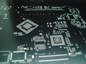
Introduction to PCB Stencils
A PCB stencil is a thin sheet of metal or plastic with precisely cut openings that correspond to the pads on a printed circuit board (PCB). These stencils are used in the PCB assembly process to apply solder paste onto the pads before placing components. The accuracy and quality of the stencil directly impact the success of the soldering process and the overall functionality of the PCB.
Advantages of Using PCB Stencils
- Precise solder paste application
- Consistent solder joint quality
- Increased production efficiency
- Cost-effective for high-volume manufacturing
Types of PCB Stencils
There are several types of PCB stencils available, each with its own advantages and disadvantages.
1. Laser-cut Stencils
Laser-cut stencils are created using a high-precision laser to cut openings in a thin sheet of stainless steel. These stencils offer excellent accuracy and durability, making them suitable for high-volume production runs.
2. Chemical-etched Stencils
Chemical-etched stencils are made by chemically etching the openings into a thin sheet of stainless steel. While not as precise as laser-cut stencils, they are more cost-effective for lower-volume production or prototyping.
3. Electroformed Stencils
Electroformed stencils are created by electroplating nickel onto a photoresist-patterned master. These stencils offer high precision and are suitable for fine-pitch applications, but they are more expensive than laser-cut or chemical-etched stencils.

PCB Stencil Making Process
The PCB stencil making process involves several steps to ensure the highest quality and accuracy.
Step 1: Design Preparation
- Review the PCB design files (Gerber or ODB++) for accuracy and completeness.
- Check the solder mask opening sizes and pad dimensions.
- Verify the stencil thickness based on the PCB design and component requirements.
Step 2: Material Selection
- Choose the appropriate stencil material (stainless steel, nickel, or polyester) based on the PCB design and production requirements.
- Select the correct stencil thickness (typically 100-150 μm for standard PCBs, or 50-80 μm for fine-pitch designs).
Step 3: Stencil Fabrication
- Transfer the stencil design to the chosen fabrication method (laser cutting, chemical etching, or electroforming).
- Cut or etch the openings in the stencil material according to the design.
- Inspect the stencil for accuracy and quality.
Step 4: Post-processing
- Clean the stencil to remove any debris or residue from the fabrication process.
- Apply a nanocoating to the stencil surface to improve solder paste release and prevent oxidation.
- Package the stencil for shipping or storage.

Stencil Design Considerations
When designing a PCB stencil, several factors must be considered to ensure optimal performance.
1. Aperture Size and Shape
The aperture size and shape should be optimized based on the pad size, pitch, and component type. Common aperture shapes include square, circular, and home plate.
| Component Type | Pitch (mm) | Aperture Size (mm) | Aperture Shape |
|---|---|---|---|
| Chip Resistor | 0.5 | 0.4 x 0.5 | Rectangle |
| QFP | 0.8 | 0.6 x 0.6 | Square |
| BGA | 1.0 | 0.8 (diameter) | Circle |
2. Stencil Thickness
The stencil thickness should be selected based on the desired solder paste volume and the PCB design. Thicker stencils deposit more solder paste, which is suitable for larger components or higher-volume production.
| PCB Type | Stencil Thickness (μm) |
|---|---|
| Standard | 100-150 |
| Fine-pitch | 80-100 |
| Ultra-fine pitch | 50-80 |
3. Aperture Wall Angle
The aperture wall angle affects the release of solder paste from the stencil. A trapezoidal aperture with a wall angle of 5-15 degrees is recommended for optimal paste release.
4. Fiducial Marks
Fiducial marks should be included in the stencil design to facilitate proper alignment between the stencil and the PCB during the solder paste printing process.

Stencil Maintenance and Cleaning
Proper maintenance and cleaning of PCB stencils are essential for ensuring consistent solder paste printing quality and extending the stencil’s lifespan.
1. Cleaning Frequency
Stencils should be cleaned regularly to prevent solder paste buildup and contamination. The cleaning frequency depends on the production volume and the type of solder paste used.
| Production Volume | Cleaning Frequency |
|---|---|
| High | Every 4-8 hours |
| Medium | Every 8-16 hours |
| Low | Every 16-24 hours |
2. Cleaning Methods
There are two primary methods for cleaning PCB stencils:
- Manual cleaning using solvents and wiping materials
- Automated cleaning using stencil cleaning machines
Manual cleaning is suitable for low-volume production or quick maintenance between prints, while automated cleaning is more efficient for high-volume production and thorough stencil cleaning.
3. Stencil Storage
When not in use, PCB stencils should be stored properly to prevent damage and contamination. Store stencils in a clean, dry environment, and use protective covers or containers to minimize exposure to dust and moisture.
Frequently Asked Questions (FAQ)
1. What is the most common material used for PCB stencils?
The most common material used for PCB stencils is stainless steel, as it offers excellent durability, stability, and precision.
2. How do I choose the right stencil thickness for my PCB design?
The stencil thickness should be selected based on the PCB design, component types, and desired solder paste volume. Generally, thicker stencils (100-150 μm) are used for standard PCBs, while thinner stencils (50-80 μm) are used for fine-pitch designs.
3. Can I reuse a PCB stencil?
Yes, PCB stencils can be reused multiple times with proper cleaning and maintenance. However, stencils will eventually wear out and need to be replaced to maintain optimal solder paste printing quality.
4. How often should I clean my PCB stencil?
The cleaning frequency depends on the production volume and the type of solder paste used. High-volume production may require cleaning every 4-8 hours, while low-volume production may only need cleaning every 16-24 hours.
5. How should I store my PCB stencils when not in use?
PCB stencils should be stored in a clean, dry environment, using protective covers or containers to minimize exposure to dust and moisture. Proper storage helps prevent damage and contamination, extending the stencil’s lifespan.
Conclusion
PCB stencils play a crucial role in the solder paste printing process, ensuring accurate and consistent solder paste application. By understanding the different types of stencils, the stencil making process, and the key design considerations, you can optimize your PCB assembly process and achieve the highest quality solder joints. Regular maintenance and cleaning of PCB stencils are essential for maintaining optimal performance and extending the stencil’s lifespan.


Leave a Reply