What is PCB Impedance and Why Does it Matter?
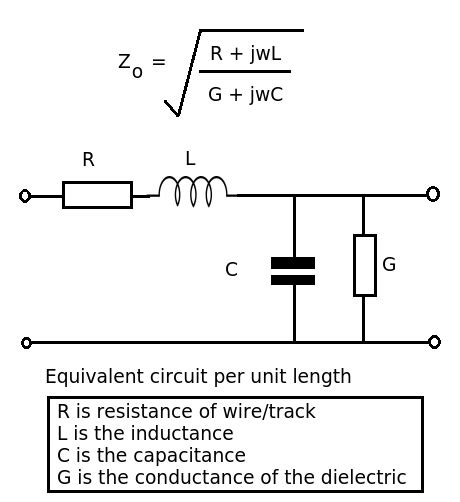
Printed circuit board (PCB) impedance refers to the opposition to alternating current (AC) in a PCB trace or transmission line. It is a critical parameter in high-speed digital and RF circuit design, as it affects signal integrity, power integrity, and electromagnetic compatibility (EMC) of the system.
PCB impedance is determined by several factors, including:
- Trace width and thickness
- Dielectric material properties (relative permittivity and loss tangent)
- Spacing between traces and reference planes (ground or power)
- Frequency of the signal
Maintaining controlled impedance is essential to ensure proper signal propagation, minimize reflections, and reduce crosstalk between traces. Mismatched impedances can lead to signal distortion, overshoot, undershoot, and ringing, which can compromise the performance and reliability of the system.
Types of PCB Impedance
There are two main types of PCB impedance:
-
Characteristic Impedance (Z0): This is the intrinsic impedance of a transmission line, determined by its geometry and dielectric properties. It is the ratio of the voltage to the current in a single-ended trace or the ratio of the differential voltage to the differential current in a differential pair. Common characteristic impedance values for PCBs are 50Ω, 75Ω, and 100Ω.
-
Differential Impedance (Zdiff): This is the impedance between two traces in a differential pair, which carry complementary signals (180° out of phase). Differential signaling is widely used in high-speed interfaces like USB, HDMI, and Ethernet to reduce electromagnetic interference (EMI) and improve noise immunity. Typical differential impedance values range from 90Ω to 120Ω.

PCB Impedance Calculation Methods
There are several methods to calculate PCB impedance, depending on the trace geometry and the desired accuracy:
1. Analytical Formulas
Analytical formulas provide a quick and easy way to estimate PCB impedance based on trace dimensions and dielectric properties. These formulas are derived from transmission line theory and assume ideal conditions (uniform cross-section, homogeneous dielectric, etc.).
Some common analytical formulas for PCB impedance are:
Microstrip Line
Z0 = (87/√(ε_r + 1.41)) * ln(5.98*h/(0.8*w + t))
Where:
– Z0 is the characteristic impedance (Ω)
– ε_r is the relative permittivity of the dielectric
– h is the dielectric thickness (mm)
– w is the trace width (mm)
– t is the trace thickness (mm)
Stripline
Z0 = (60/√ε_r) * ln(4*h/(0.67*π*(0.8*w + t)))
Where:
– Z0 is the characteristic impedance (Ω)
– ε_r is the relative permittivity of the dielectric
– h is the dielectric thickness (mm)
– w is the trace width (mm)
– t is the trace thickness (mm)
Coplanar Waveguide
Z0 = (30*π/√ε_eff) * K(k)/K(k')
Where:
– Z0 is the characteristic impedance (Ω)
– ε_eff is the effective relative permittivity
– K(k) and K(k’) are complete elliptic integrals of the first kind
– k = S/(S + 2*w)
– k’ = √(1 – k^2)
– S is the spacing between traces (mm)
– w is the trace width (mm)
Analytical formulas provide a good starting point for PCB impedance design, but they have limitations:
- They assume ideal conditions that may not hold in practice (e.g., non-uniform cross-section, anisotropic dielectric)
- They do not account for frequency-dependent effects (dispersion, loss)
- They may not be accurate for complex geometries or multiple dielectric layers
2. Numerical Simulations
Numerical simulations provide a more accurate and flexible way to calculate PCB impedance, by solving Maxwell’s equations in the frequency or time domain. These simulations can handle arbitrary trace geometries, multiple dielectric layers, and frequency-dependent material properties.
Some popular numerical simulation methods for PCB impedance are:
Finite Element Method (FEM)
FEM is a frequency-domain method that discretizes the PCB structure into small elements (triangles or tetrahedra) and solves for the electric and magnetic fields at each node. FEM is well-suited for complex geometries and inhomogeneous materials, but it can be computationally expensive for large problems.
Finite Difference Time Domain (FDTD)
FDTD is a time-domain method that discretizes the PCB structure into a regular grid (Yee cell) and solves for the electric and magnetic fields at each time step. FDTD is efficient for broadband simulations and can handle nonlinear and dispersive materials, but it requires fine meshing for curved geometries.
Method of Moments (MoM)
MoM is a frequency-domain method that solves the integral form of Maxwell’s equations by dividing the PCB structure into segments and calculating the currents and charges on each segment. MoM is accurate for thin traces and open boundaries, but it can be memory-intensive for large problems.
Numerical simulations provide the most accurate and flexible way to calculate PCB impedance, but they require specialized software (e.g., ANSYS HFSS, CST Studio Suite, Keysight ADS) and expertise. They are typically used for critical signal paths, high-speed interfaces, and complex PCB stackups.
3. Empirical Measurements
Empirical measurements provide a direct way to verify PCB impedance, by using a time-domain reflectometer (TDR) or a vector network analyzer (VNA). These instruments send a high-frequency signal through the PCB trace and measure the reflected or transmitted signal to calculate the impedance.
TDR measurements are performed in the time domain and provide a spatial profile of the impedance along the trace. They are useful for identifying impedance discontinuities, such as vias, connectors, or layer transitions.
VNA measurements are performed in the frequency domain and provide the scattering parameters (S-parameters) of the PCB trace. They are useful for characterizing the frequency response, insertion loss, and return loss of the trace.
Empirical measurements are the most accurate way to verify PCB impedance, but they require physical access to the PCB and specialized equipment. They are typically used for prototype validation, quality control, and troubleshooting.

PCB Impedance Calculator Tools
There are several PCB impedance calculator tools available, ranging from simple web-based calculators to advanced simulation software. Some popular options are:
Web-Based Calculators
- EEWeb PCB Impedance Calculator: A free online calculator for microstrip, stripline, and coplanar waveguide impedance, based on analytical formulas.
- Microstrip Impedance Calculator: A free online calculator for microstrip impedance, with options for substrate material, trace dimensions, and frequency.
- Multi-Layer PCB Stackup and Impedance Calculator: A web-based calculator for multi-layer PCB stackup and impedance, with options for dielectric materials, layer thicknesses, and via geometry.
Spreadsheet Calculators
- EEWeb PCB Impedance Spreadsheet: An Excel spreadsheet for calculating microstrip, stripline, and coplanar waveguide impedance, based on analytical formulas.
- Polar Si9000 Impedance Calculator: An Excel spreadsheet for calculating microstrip, stripline, and coplanar waveguide impedance, with options for substrate material, trace dimensions, and frequency.
Software Tools
- ANSYS HFSS: A 3D electromagnetic simulation software for high-frequency PCB and antenna design, with advanced impedance calculation and optimization capabilities.
- CST Studio Suite: A 3D electromagnetic simulation software for PCB, RF, and EMC design, with time-domain and frequency-domain solvers for impedance calculation.
- Keysight ADS: A circuit and system simulation software for PCB, RF, and high-speed digital design, with built-in impedance calculators and optimization tools.
- Altium Designer: A PCB design software with integrated impedance calculation and control features, based on analytical formulas and material libraries.
- Cadence Allegro PCB Designer: A PCB design software with built-in impedance calculators and constraint managers, supporting multiple routing layers and differential pairs.

FAQ
1. What is the difference between single-ended and differential impedance?
Single-ended impedance refers to the characteristic impedance of a single trace with respect to a reference plane (ground or power), while differential impedance refers to the impedance between two traces in a differential pair, which carry complementary signals. Single-ended impedance is important for signal integrity, while differential impedance is important for noise immunity and EMI reduction.
2. What is the typical impedance of a USB interface?
USB interfaces (USB 2.0 and USB 3.x) use differential signaling with a nominal differential impedance of 90Ω ± 10%. This means that the PCB traces for USB data lines (D+ and D-) should be designed to have a differential impedance close to 90Ω, to ensure proper signal quality and minimize reflections.
3. How does PCB thickness affect impedance?
PCB thickness (or dielectric thickness) has a significant effect on impedance, as it determines the spacing between the trace and the reference plane. In general, thicker PCBs have higher characteristic impedance, as the increased spacing reduces the capacitance between the trace and the plane. Conversely, thinner PCBs have lower characteristic impedance, as the reduced spacing increases the capacitance.
4. What is the impact of trace width on PCB impedance?
Trace width is another important factor in PCB impedance, as it affects both the inductance and capacitance of the trace. Wider traces have lower characteristic impedance, as they have higher capacitance and lower inductance per unit length. Narrower traces have higher characteristic impedance, as they have lower capacitance and higher inductance per unit length. Therefore, adjusting the trace width is a common way to control PCB impedance, within the limits of manufacturing constraints and current carrying capacity.
5. What is the role of dielectric constant in PCB impedance?
The dielectric constant (or relative permittivity) of the PCB material is another key factor in impedance, as it determines the speed of propagation and the capacitance of the trace. Higher dielectric constants result in lower characteristic impedance, as they increase the capacitance between the trace and the reference plane. Lower dielectric constants result in higher characteristic impedance, as they reduce the capacitance. Common PCB materials, such as FR-4, have dielectric constants in the range of 4.0 to 4.5, while low-loss materials, such as Rogers RO4003C, have lower dielectric constants around 3.4.
Conclusion
PCB impedance is a critical parameter in high-speed digital and RF circuit design, as it affects signal integrity, power integrity, and EMC of the system. Calculating and controlling PCB impedance requires knowledge of transmission line theory, PCB materials, and manufacturing constraints.
There are several methods to calculate PCB impedance, including analytical formulas, numerical simulations, and empirical measurements. Each method has its own advantages and limitations, depending on the complexity of the design and the desired accuracy.
PCB designers can use various impedance calculator tools, ranging from web-based calculators to advanced simulation software, to aid in the design and optimization of controlled impedance traces.
By understanding the principles and tools of PCB impedance calculation, designers can ensure proper signal propagation, minimize reflections and crosstalk, and improve the overall performance and reliability of their PCB designs.


Leave a Reply