Introduction to PCB Basics
Printed Circuit Boards (PCBs) are the backbone of modern electronics. They are used in almost every electronic device, from simple gadgets to complex machines. PCBs provide a means to mechanically support and electrically connect electronic components using conductive tracks, pads, and other features etched from copper sheets laminated onto a non-conductive substrate.
In this article, we will cover the basics of PCBs, including their types, manufacturing process, design considerations, and how to get started with PCB design as a beginner.
Types of PCBs
PCBs can be classified based on various factors such as the number of layers, flexibility, and material used. Here are some common types of PCBs:
Single-Layer PCBs
Single-layer PCBs have conductive tracks on only one side of the board. They are the simplest and most cost-effective type of PCB, suitable for basic electronic projects.
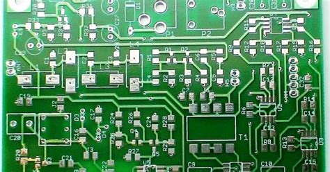
Double-Layer PCBs
Double-layer PCBs have conductive tracks on both sides of the board, allowing for more complex circuits and higher component density compared to single-layer PCBs.
Multi-Layer PCBs
Multi-layer PCBs have three or more conductive layers, with insulating layers sandwiched between them. They are used for complex electronic devices that require high component density and signal integrity.
| PCB Type | Layers | Cost | Complexity |
|---|---|---|---|
| Single-Layer | 1 | Low | Simple |
| Double-Layer | 2 | Medium | Moderate |
| Multi-Layer | 3+ | High | Complex |
Flexible PCBs
Flexible PCBs are made from flexible materials, such as polyimide, allowing them to bend and conform to various shapes. They are often used in wearable electronics and applications where space is limited.
Rigid-Flex PCBs
Rigid-flex PCBs combine the features of both rigid and flexible PCBs, with rigid sections for mounting components and flexible sections for connecting them. They offer the benefits of both types of PCBs in a single board.

PCB Manufacturing Process
The PCB manufacturing process involves several steps, from design to final assembly. Here’s an overview of the process:
PCB Design
The first step in PCB manufacturing is designing the circuit schematic and layout using PCB design software. The design must adhere to various design rules and guidelines to ensure manufacturability and functionality.
PCB Fabrication
Once the design is complete, the PCB is fabricated using the following steps:
- Printing the circuit pattern onto the copper-clad board using photoresist.
- Etching away the unwanted copper, leaving only the desired circuit pattern.
- Drilling holes for through-hole components and vias.
- Applying a solder mask to protect the copper traces and prevent short circuits.
- Applying a silkscreen layer for component labels and other markings.
PCB Assembly
After fabrication, the PCB is assembled with electronic components using one of two methods:
- Through-hole assembly: Components are inserted into drilled holes and soldered onto the board.
- Surface-mount assembly: Components are placed on pads on the surface of the board and soldered using reflow or wave soldering techniques.
PCB Testing
The assembled PCB undergoes various tests to ensure functionality and reliability, such as:
- Visual inspection
- Automated optical inspection (AOI)
- In-circuit testing (ICT)
- Functional testing

PCB Design Considerations
When designing a PCB, there are several factors to consider to ensure optimal performance and manufacturability. Some key considerations include:
Component Placement
Components should be placed in a logical and efficient manner, taking into account factors such as signal integrity, heat dissipation, and mechanical constraints.
Trace Routing
Traces should be routed to minimize signal interference, crosstalk, and electromagnetic interference (EMI). Proper trace width and spacing should be maintained based on the current and voltage requirements.
Power and Ground Planes
Adequate power and ground planes should be incorporated into the design to ensure stable power delivery and reduce noise.
Thermal Management
Proper thermal management techniques, such as the use of heatsinks and thermal vias, should be employed to dissipate heat generated by components.
Manufacturing Constraints
The design should adhere to the manufacturing capabilities of the chosen PCB fabrication and assembly vendor, such as minimum trace width, hole size, and clearances.

Getting Started with PCB Design
As a beginner, getting started with PCB design may seem daunting. However, with the right tools and resources, you can quickly learn the basics and start designing your own PCBs. Here are some steps to get started:
Learn the Basics
Start by learning the fundamentals of electronics and PCB design. There are many online resources, such as tutorials, articles, and videos, that can help you understand the basics.
Choose a PCB Design Software
There are many PCB design software options available, ranging from free open-source tools to professional-grade commercial software. Some popular options for beginners include:
| Software | License | Ease of Use | Features |
|---|---|---|---|
| KiCad | Open-source | Beginner-friendly | Schematic capture, PCB layout, 3D viewer |
| EasyEDA | Free/Commercial | Beginner-friendly | Web-based, schematic capture, PCB layout, simulation |
| Eagle | Commercial | Moderate | Schematic capture, PCB layout, extensive component libraries |
| Altium Designer | Commercial | Advanced | Schematic capture, PCB layout, simulation, high-end features |
Practice with Simple Projects
Start with simple projects, such as LED blinkers or small sensor circuits, to gain hands-on experience with PCB design. As you become more comfortable, gradually move on to more complex projects.
Join Communities and Seek Guidance
Join online communities, forums, and social media groups dedicated to PCB design and electronics. These communities can provide valuable advice, inspiration, and support as you learn and grow.
Frequently Asked Questions (FAQ)
- What is the difference between a schematic and a PCB layout?
-
A schematic is a symbolic representation of an electronic circuit, showing the components and their interconnections. A PCB layout is the physical design of the PCB, showing the actual placement of components and the routing of traces.
-
What is the purpose of a solder mask on a PCB?
-
A solder mask is a protective layer applied to the PCB to prevent short circuits and protect the copper traces from oxidation and damage. It also helps to prevent solder bridges during the assembly process.
-
What is the difference between through-hole and surface-mount components?
-
Through-hole components have leads that are inserted into drilled holes in the PCB and soldered on the opposite side. Surface-mount components are placed directly on pads on the surface of the PCB and soldered using reflow or wave soldering techniques.
-
How do I choose the right PCB fabrication and assembly vendor?
-
When choosing a PCB fabrication and assembly vendor, consider factors such as their manufacturing capabilities, turnaround time, cost, quality control, and customer support. Read reviews and ask for recommendations from experienced designers or community members.
-
What are some common mistakes to avoid when designing PCBs?
- Some common mistakes to avoid include: not adhering to design rules and guidelines, improper component placement, incorrect trace routing, inadequate power and ground planes, and not considering manufacturing constraints. Always double-check your design and seek feedback from experienced designers before sending it for fabrication.
Conclusion
PCBs are essential components in modern electronics, and understanding their basics is crucial for anyone interested in electronic design. By learning about PCB types, manufacturing processes, design considerations, and getting hands-on experience with PCB design software, beginners can quickly get started on their journey to creating functional and reliable electronic devices.
Remember to start with simple projects, seek guidance from experienced designers and communities, and continuously learn and improve your skills. With dedication and practice, you can master the art of PCB design and bring your electronic ideas to life.


Leave a Reply