Understanding PCB Panel Requirements for Efficient Assembly
What are PCB Panels?
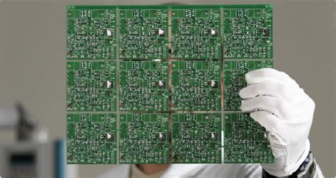
Printed Circuit Board (PCB) panels, also known as PCB arrays, are large boards containing multiple identical PCB Designs arranged in a matrix. These panels are used in the PCB Assembly process to increase efficiency and reduce manufacturing costs. By producing several PCBs simultaneously on a single panel, manufacturers can optimize material usage, minimize handling, and streamline the assembly process.
Key Factors in PCB Panel Design
When designing PCB panels for assembly, several key factors must be considered to ensure optimal results:
-
Panel Size: The panel size should be compatible with the manufacturing equipment and processes. Standard panel sizes include 18″ x 24″, 21″ x 24″, and 18″ x 21″, but custom sizes can be accommodated based on specific requirements.
-
Board Orientation: The orientation of the individual PCBs on the panel should be consistent and aligned to facilitate automated assembly processes. Proper orientation also helps minimize material waste and ensures accurate placement of components.
-
Spacing and Clearance: Adequate spacing between individual PCBs on the panel is crucial to prevent damage during the assembly process. A minimum spacing of 0.125″ to 0.25″ is typically recommended, depending on the complexity of the design and the assembly equipment used.
-
Fiducial Markers: Fiducial markers are reference points placed on the panel to help align and orient the board during the assembly process. These markers should be clearly visible and positioned accurately to ensure precise component placement.
-
Tooling Holes: Tooling holes are used to secure the panel during the assembly process. The size, location, and quantity of tooling holes should be specified based on the manufacturing equipment and panel dimensions.
Benefits of Using PCB Panels in Assembly
Using PCB panels in the assembly process offers several significant advantages:
-
Increased Efficiency: Producing multiple PCBs on a single panel reduces handling time and speeds up the assembly process. Automated assembly equipment can process panels more quickly than individual boards, resulting in higher throughput and lower production costs.
-
Improved Accuracy: Panel-based assembly ensures consistent placement of components across all boards in the panel. This uniformity minimizes the risk of errors and improves the overall quality of the assembled PCBs.
-
Reduced Material Waste: By arranging multiple PCBs on a single panel, manufacturers can optimize material usage and minimize waste. This is particularly beneficial for designs with irregular shapes or small form factors.
-
Cost Savings: The increased efficiency and reduced material waste associated with panel-based assembly translate into significant cost savings. Manufacturers can produce a higher volume of PCBs in less time, reducing labor costs and increasing profitability.
PCB Panel Material Selection
The choice of material for PCB panels depends on several factors, including the intended application, environmental conditions, and manufacturing requirements. Common materials used for PCB panels include:
-
FR-4: FR-4 is a fire-resistant epoxy laminate material widely used in PCB Manufacturing. It offers good mechanical and electrical properties, making it suitable for a wide range of applications.
-
Aluminum: Aluminum PCB panels are used in applications requiring excellent thermal dissipation, such as high-power electronics or LED lighting. The metal substrate helps dissipate heat efficiently, improving the performance and longevity of the assembled PCBs.
-
Flexible Materials: Flexible PCB panels, made from materials like polyimide or polyester, are used in applications requiring bendable or conformable circuits. These panels are ideal for wearable electronics, medical devices, and compact electronic assemblies.
PCB Panel Thickness Considerations
The thickness of PCB panels is an important factor in the assembly process. Thinner panels are more flexible and easier to handle, while thicker panels offer greater rigidity and stability. The choice of panel thickness depends on the specific requirements of the PCB design and the assembly equipment used.
Common PCB panel thicknesses include:
| Thickness | Application |
|---|---|
| 0.031″ (0.8mm) | Thin, flexible circuits |
| 0.062″ (1.6mm) | Standard thickness for most applications |
| 0.093″ (2.4mm) | Thicker boards for increased rigidity |
| 0.125″ (3.2mm) | Heavy-duty applications or high-layer count boards |
PCB Panel Layout and Panelization Techniques
Effective PCB panel layout and panelization techniques are crucial for successful assembly. Some key considerations include:
-
Board Orientation: PCBs should be oriented on the panel to maximize material utilization and minimize waste. Consistent orientation also facilitates automated assembly processes.
-
Panelization Methods: There are several methods for panelizing PCBs, including tab routing, scoring, and perforation. The choice of method depends on the specific requirements of the design and the assembly process.
-
Copper Balancing: Copper balancing involves ensuring an even distribution of copper on both sides of the panel to prevent warping during the manufacturing process. This is particularly important for designs with high copper coverage or asymmetrical layouts.
-
Depaneling Techniques: Depaneling refers to the process of separating individual PCBs from the panel after assembly. Common depaneling techniques include routing, punching, and v-scoring. The choice of technique depends on the panel material, thickness, and the requirements of the end application.
Testing and Inspection of PCB Panels
To ensure the quality and reliability of assembled PCBs, testing and inspection of PCB panels are critical steps in the manufacturing process. Some common testing and inspection techniques include:
-
Automated Optical Inspection (AOI): AOI systems use high-resolution cameras and advanced algorithms to detect surface-level defects, such as missing components, incorrect placement, or solder bridging.
-
X-Ray Inspection: X-ray inspection is used to detect internal defects, such as voids in solder joints or misaligned components. This technique is particularly useful for inspecting high-density or multi-layer PCBs.
-
Electrical Testing: Electrical testing, such as continuity testing and in-circuit testing, verifies the electrical functionality of the assembled PCBs. These tests help identify short circuits, open circuits, or other electrical faults.
-
Functional Testing: Functional testing involves subjecting the assembled PCBs to real-world operating conditions to ensure they perform as intended. This may include environmental testing, such as temperature cycling or vibration testing, depending on the end application.
Frequently Asked Questions (FAQ)
-
What is the minimum spacing required between PCBs on a panel?
The minimum spacing between PCBs on a panel typically ranges from 0.125″ to 0.25″, depending on the complexity of the design and the assembly equipment used. Adequate spacing is essential to prevent damage during the assembly process. -
Can custom panel sizes be accommodated in PCB assembly?
Yes, custom panel sizes can be accommodated based on specific requirements. However, it is important to ensure that the panel size is compatible with the manufacturing equipment and processes to avoid any issues during assembly. -
What are the benefits of using aluminum PCB panels?
Aluminum PCB panels offer excellent thermal dissipation properties, making them ideal for applications that generate significant heat, such as high-power electronics or LED lighting. The metal substrate helps dissipate heat efficiently, improving the performance and longevity of the assembled PCBs. -
How does copper balancing help in PCB panel manufacturing?
Copper balancing involves ensuring an even distribution of copper on both sides of the panel to prevent warping during the manufacturing process. This is particularly important for designs with high copper coverage or asymmetrical layouts. Proper copper balancing helps maintain the flatness and stability of the panel, reducing the risk of defects or assembly issues. -
What is the purpose of functional testing in PCB assembly?
Functional testing involves subjecting the assembled PCBs to real-world operating conditions to ensure they perform as intended. This may include environmental testing, such as temperature cycling or vibration testing, depending on the end application. Functional testing helps identify any performance issues or reliability concerns before the PCBs are deployed in the final product.
Conclusion
PCB panel requirements play a crucial role in ensuring efficient and cost-effective PCB assembly. By understanding the key factors in panel design, material selection, thickness considerations, layout techniques, and testing methods, manufacturers can optimize their assembly processes and produce high-quality PCBs consistently.
Effective panel design and management not only streamline the assembly process but also contribute to reduced material waste, increased accuracy, and significant cost savings. As PCB designs continue to evolve and become more complex, staying up-to-date with the latest panel requirements and best practices is essential for manufacturers to remain competitive in the industry.
By adhering to the panel requirements outlined in this article and working closely with experienced PCB assembly providers, designers and engineers can ensure their PCB projects are successfully brought to life, meeting the highest standards of quality and reliability.


Leave a Reply