Understanding PCB etching
Before we dive into the process of testing your etching chops, let’s first understand what PCB etching entails. PCB etching is a subtractive manufacturing method where a chemical solution, known as an etchant, is used to remove the unwanted copper from a copper-clad board, leaving behind the desired conductive traces that form the circuit.
Types of PCB Etching
There are two main types of PCB etching:
-
Chemical Etching: This method involves submerging the PCB in a chemical solution, such as ferric chloride or ammonium persulfate, which selectively dissolves the exposed copper.
-
Mechanical Etching: In this method, a CNC machine or a milling machine is used to physically remove the unwanted copper from the board.
For the purpose of this article, we will focus on chemical etching, as it is the most common and accessible method for hobbyists and beginners.
Materials and Tools Required
Before you start your PCB etching journey, make sure you have the following materials and tools:
- Copper-clad board (single or double-sided, depending on your project)
- Etchant solution (ferric chloride or ammonium persulfate)
- Etching tank or container
- Latex or nitrile gloves
- Safety goggles
- Apron or protective clothing
- Plastic tweezers or tongs
- Permanent marker or etch-resistant pen
- Rubbing alcohol or acetone
- Drill or Dremel tool (for drilling holes)
- Sandpaper or scouring pad
- Multimeter (for testing continuity)

Designing Your PCB
The first step in creating a PCB is designing the circuit layout. You can use various PCB design software, such as KiCad, Eagle, or Altium Designer, to create your schematic and lay out the components on the board.
When designing your PCB, consider the following factors:
- Component placement and orientation
- Trace width and spacing
- Ground planes and power planes
- Via placement and size
- Clearance between components and traces
Once you have finalized your PCB design, export the design files in a format compatible with your chosen etching method (e.g., Gerber files for chemical etching).

Preparing the Copper-Clad Board
Before you start etching, you need to prepare the copper-clad board. Follow these steps:
-
Clean the copper surface using rubbing alcohol or acetone to remove any grease or dirt.
-
If your design includes through-hole components, drill the necessary holes using a drill or Dremel tool.
-
Apply the etch-resistant pattern to the copper surface using one of the following methods:
- Use a permanent marker or etch-resistant pen to draw the circuit pattern directly on the copper.
- Print the circuit pattern on a laser printer and use the toner transfer method to transfer the pattern onto the copper.
-
Use photoresist and expose the board to UV light through a transparency with the circuit pattern.
-
Inspect the board for any defects or errors in the pattern. Make corrections if necessary.

Etching the PCB
Now that your board is prepared, it’s time to start the etching process. Follow these steps:
-
Put on your gloves, safety goggles, and protective clothing.
-
In a well-ventilated area, pour the etchant solution into the etching tank or container. Make sure the solution is deep enough to cover the entire board.
-
Carefully submerge the prepared board into the etchant solution using plastic tweezers or tongs.
-
Agitate the board gently to ensure even etching and prevent air bubbles from forming on the surface.
-
Monitor the etching process closely. The time required for etching depends on the strength of the etchant solution, the thickness of the copper, and the ambient temperature. Typically, it takes between 10 to 30 minutes.
-
Once the unwanted copper has been completely removed, remove the board from the etchant solution using the tweezers or tongs.
-
Rinse the board thoroughly with water to remove any remaining etchant.
-
Remove the etch-resistant pattern using sandpaper or a scouring pad.
-
Clean the board with rubbing alcohol or acetone to remove any residue.
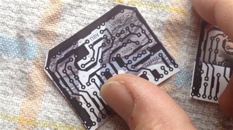
Testing the PCB
After etching, it’s crucial to test your PCB to ensure proper functionality and identify any potential issues. Here are some tests you can perform:
Visual Inspection
Visually inspect the PCB for any visible defects, such as:
- Incomplete or over-etched traces
- Shorts or bridges between traces
- Damage to the board surface
- Misaligned or missing holes
If you spot any issues, you may need to rework the board or start over with a new one.
Continuity Test
Use a multimeter to test the continuity of the traces and connections on your PCB. Set the multimeter to the continuity or resistance mode and follow these steps:
-
Place one probe on one end of a trace and the other probe on the other end.
-
The multimeter should indicate continuity (usually by beeping or displaying a low resistance value) if the trace is intact.
-
Repeat this process for all traces and connections on the board.
If you find any open circuits or high resistance values, investigate the issue and repair the board if possible.
Power-On Test
Once you have confirmed the continuity of your PCB, it’s time to test it with power. Follow these steps:
-
Solder the components onto the PCB according to your schematic.
-
Double-check the component placement and orientation.
-
Apply power to the board, starting with a low voltage if possible.
-
Use a multimeter to measure the voltage levels at various points on the board and compare them with your expected values.
-
Test the functionality of your circuit by applying inputs and measuring outputs.
If your PCB passes the power-on test, congratulations! You have successfully etched and tested your PCB.
Tips and Tricks
Here are some additional tips and tricks to help you achieve better results when etching PCBs:
- Always work in a well-ventilated area and wear proper protective gear when handling etchant solutions.
- Use fresh etchant solution for each board to ensure consistent etching results.
- Experiment with different etching times and agitation methods to find the optimal settings for your setup.
- If you’re working with double-sided boards, make sure to align the patterns on both sides accurately.
- Use a fiberglass pen or a small brush to touch up any minor defects or breaks in the traces.
- Consider using solder mask and silkscreen to enhance the durability and aesthetics of your PCB.
FAQ
-
Can I reuse the etchant solution?
While it’s possible to reuse the etchant solution, it’s generally not recommended. The etching process depletes the solution, and reusing it may lead to inconsistent results or longer etching times. It’s best to dispose of the used solution properly and use fresh etchant for each board. -
How do I dispose of the used etchant solution?
Etchant solutions, such as ferric chloride or ammonium persulfate, are considered hazardous waste and should be disposed of according to local regulations. Contact your local waste management authority for guidance on proper disposal methods. Never pour the solution down the drain or into the environment. -
Can I etch PCBs without using a chemical solution?
Yes, there are alternative methods for etching PCBs that don’t involve chemical solutions. One popular method is mechanical etching, where a CNC machine or a milling machine is used to remove the unwanted copper. Another option is to use a laser engraver to burn away the copper. However, these methods require specialized equipment and may not be as accessible for beginners. -
What should I do if I accidentally over-etch my PCB?
If you’ve over-etched your PCB and the traces are too thin or have breaks, you can try to repair them using a fiberglass pen or a small brush and conductive paint or ink. Carefully apply the conductive material to the affected areas and allow it to dry completely before testing the board again. If the damage is extensive, you may need to start over with a new board. -
Can I use the same design files for different etching methods?
In most cases, yes. The design files used for PCB etching, such as Gerber files, are standardized and can be used with various etching methods. However, it’s essential to check the requirements of your chosen etching method and make sure your design files are compatible. Some etching services may have specific guidelines or limitations that you need to follow.
Conclusion
Testing your etching chops and creating a PCB map is an exciting and rewarding process that allows you to bring your electronic projects to life. By following the steps outlined in this guide, you can successfully design, etch, and test your own custom PCBs.
Remember to prioritize safety, work in a well-ventilated area, and wear proper protective gear when handling etchant solutions. Take your time, be patient, and don’t be discouraged if your first attempts aren’t perfect. With practice and perseverance, you’ll soon be etching PCBs like a pro!
Happy etching!
| Step | Description |
|---|---|
| 1 | Design your PCB using PCB design software |
| 2 | Prepare the copper-clad board by cleaning and drilling holes |
| 3 | Apply the etch-resistant pattern to the copper surface |
| 4 | Etch the PCB in the etchant solution |
| 5 | Rinse the board and remove the etch-resistant pattern |
| 6 | Test the PCB for continuity and functionality |


Leave a Reply