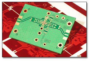
Understanding the PCB prototyping Process
Before we dive into the methods of accelerating PCB prototyping, let’s first understand the basic steps involved in the process:
- Design: Create the schematic and layout of the PCB using CAD software.
- Fabrication: Manufacture the physical PCB based on the design files.
- Assembly: Solder components onto the fabricated PCB.
- Testing: Verify the functionality and performance of the assembled PCB.
Each of these steps can be optimized to reduce the overall prototyping time.
Rapid Prototyping Techniques
3D Printing
3D printing has revolutionized the way we create physical objects, including PCBs. By using conductive filaments or inks, it is possible to 3D print functional PCBs in a matter of hours. This method is particularly useful for simple designs or quick proof-of-concept prototypes.
Advantages:
– Fast turnaround time
– Low cost for small quantities
– Ability to create complex shapes and structures
Disadvantages:
– Limited resolution and conductivity compared to traditional PCBs
– Not suitable for high-frequency or high-power applications
PCB Milling
PCB milling is a subtractive manufacturing process that uses a computer-controlled milling machine to remove copper from a pre-laminated PCB substrate. This method is faster than traditional etching processes and allows for quick iterations of PCB designs.
Advantages:
– Faster than etching processes
– Ability to create prototypes in-house
– Suitable for low-volume production
Disadvantages:
– Limited to double-sided PCBs
– Requires specialized equipment and skills
Rapid PCB Fabrication Services
Many PCB fabrication companies now offer rapid prototyping services with turnaround times as short as 24 hours. These services utilize advanced manufacturing techniques and prioritize prototype orders to deliver quick results.
Advantages:
– Fast turnaround times
– Professional-grade PCBs
– Wide range of materials and specifications available
Disadvantages:
– Higher cost compared to slower production methods
– Minimum order quantities may apply

Optimizing the Design Process
Using Pre-Designed Modules
Incorporating pre-designed and tested modules, such as microcontroller boards, wireless communication modules, or power management units, can significantly speed up the design process. These modules have already been optimized for performance and reliability, reducing the time spent on designing and testing these components from scratch.
Advantages:
– Reduced design time and effort
– Improved reliability and performance
– Easier integration with existing systems
Disadvantages:
– Limited customization options
– Potentially higher cost compared to custom-designed components
Automated Design Tools
Modern PCB design software often includes automated design tools that can help streamline the design process. These tools can assist with tasks such as component placement, routing, and design rule checking, reducing the time and effort required to create a functional PCB layout.
Advantages:
– Faster design process
– Reduced risk of human error
– Improved design consistency and quality
Disadvantages:
– Learning curve associated with new software tools
– Potential limitations in terms of design flexibility

Streamlining the Assembly Process
Surface Mount Technology (SMT)
Surface Mount Technology (SMT) is a method of assembling PCBs where components are mounted directly onto the surface of the board, rather than through holes. SMT allows for smaller components, higher component density, and automated assembly processes, which can significantly reduce the time and cost of PCB assembly.
Advantages:
– Faster assembly times
– Higher component density
– Improved reliability and performance
Disadvantages:
– Requires specialized equipment and skills
– Not suitable for all component types
Automated Assembly Equipment
Investing in automated assembly equipment, such as pick-and-place machines and reflow ovens, can greatly accelerate the PCB assembly process. These machines can place components and solder them onto the PCB with high precision and speed, reducing the time and labor required for manual assembly.
Advantages:
– Fast and efficient assembly
– High precision and consistency
– Reduced labor costs
Disadvantages:
– High initial investment costs
– Requires trained operators and maintenance

Rapid Testing and Verification
In-Circuit Testing (ICT)
In-Circuit Testing (ICT) is a method of testing assembled PCBs by directly probing the individual components and interconnections. ICT systems can quickly identify manufacturing defects and component failures, reducing the time spent on manual testing and troubleshooting.
Advantages:
– Fast and comprehensive testing
– Early detection of manufacturing defects
– Automated test process
Disadvantages:
– Requires specialized test fixtures and programming
– Limited coverage for certain component types
Boundary Scan Testing
Boundary Scan Testing, also known as JTAG testing, is a method of testing digital components and interconnections on a PCB by using a special test access port (TAP). This method allows for testing of complex digital circuits without the need for physical access to individual components.
Advantages:
– Non-intrusive testing of digital components
– Ability to test complex circuits
– Automated test process
Disadvantages:
– Limited to digital components with JTAG support
– Requires specialized software and hardware tools
Case Studies
Company A: From 3 Weeks to 3 Days
Company A, a consumer electronics startup, was struggling with long PCB prototyping times that were delaying their product development cycle. By implementing a combination of 3D printing for quick prototypes, rapid PCB fabrication services for professional-grade boards, and automated design tools, they were able to reduce their prototyping time from 3 weeks to just 3 days.
Company B: Streamlining Assembly with SMT
Company B, a medical device manufacturer, was looking to streamline their PCB assembly process to meet increasing demand for their products. By transitioning from through-hole to surface mount technology (SMT) and investing in automated assembly equipment, they were able to reduce their assembly time by 75% while improving product quality and consistency.
Frequently Asked Questions (FAQ)
- What is the fastest way to create a PCB Prototype?
-
The fastest way to create a PCB prototype depends on the complexity of the design and the required specifications. For simple designs, 3D printing with conductive materials can provide prototypes in a matter of hours. For more complex designs, rapid PCB fabrication services with quick turnaround times are often the best option.
-
How much does it cost to speed up PCB prototyping?
-
The cost of speeding up PCB prototyping varies depending on the methods used. 3D printing and PCB milling can be relatively low-cost for small quantities, while rapid PCB fabrication services and automated assembly equipment require higher investments. However, the time and cost savings achieved through faster prototyping can often justify the initial expenses.
-
Can I speed up PCB prototyping without compromising quality?
-
Yes, many of the techniques and technologies discussed in this article, such as rapid PCB fabrication services, surface mount technology, and automated testing, can help speed up prototyping while maintaining or even improving the quality of the final product.
-
What skills are required to implement Rapid PCB Prototyping techniques?
-
Implementing rapid PCB prototyping techniques requires a combination of skills, including PCB design, fabrication, assembly, and testing. Familiarity with CAD software, manufacturing processes, and testing equipment is essential. However, many of these skills can be acquired through training or by collaborating with experienced professionals.
-
How do I choose the best rapid prototyping method for my project?
- Choosing the best rapid prototyping method depends on factors such as the complexity of the design, the required specifications, the available budget, and the desired turnaround time. It’s essential to evaluate each method’s advantages and disadvantages and consider the specific needs of your project. In some cases, a combination of methods may provide the best results.
Conclusion
PCB prototyping is a critical step in the development of electronic devices, but traditional methods can be time-consuming and delay product development cycles. By implementing rapid prototyping techniques such as 3D printing, PCB milling, and rapid PCB fabrication services, along with optimizing the design and assembly processes, it is possible to speed up PCB prototypes from weeks to minutes.
Investing in technologies like surface mount technology, automated assembly equipment, and advanced testing methods can further streamline the prototyping process and improve the quality and consistency of the final product.
As technology continues to advance, we can expect to see even more innovative solutions for rapid PCB prototyping, enabling designers and engineers to bring their ideas to life faster than ever before.


Leave a Reply