What is FPGA Programming?
FPGA stands for Field Programmable Gate Array. It is an integrated circuit that can be programmed and customized by the user after manufacturing. FPGAs contain an array of programmable logic blocks and a hierarchy of reconfigurable interconnects, allowing the blocks to be “wired together” to create complex digital circuits.
FPGA programming involves using hardware description languages (HDLs) like Verilog or VHDL to define the desired digital circuit behavior. This code is then synthesized, mapped, placed and routed to configure the FPGA to implement the specified logic.
Some key advantages of FPGAs compared to fixed-function chips or microcontrollers:
– Flexibility to change functionality on the fly
– Ability to implement highly parallel architectures
– Low latency and high throughput
– Deterministic timing
FPGAs are used in a wide range of applications including telecommunications, automotive, aerospace/defense, high-performance computing, artificial intelligence accelerators and more.
FPGA Programming Flow
The typical steps involved in FPGA programming are:
-
Design Entry: Describe the desired hardware functionality using Verilog, VHDL or a schematic capture tool. High-level synthesis from C/C++ is also possible.
-
Logic Synthesis: The HDL code is converted into a netlist – a description of the basic logic gates and their interconnections needed to implement the design. Synthesis tools perform hardware-specific optimizations.
-
Mapping: The synthesized netlist is mapped to the specific logic resources (LUTs, flip-flops, block RAMs, DSPs, etc.) available on the target FPGA device.
-
Placement & Routing: The mapped design is placed onto specific locations on the FPGA and interconnected using the available routing resources, while meeting timing constraints.
-
Bitstream Generation: The placed and routed design is converted into a configuration file (bitstream) that can be loaded onto the FPGA.
-
FPGA Configuration: The bitstream is loaded onto the FPGA board’s configuration memory via JTAG, flash or other interface to implement the custom logic design.
Here is a simplified diagram of the FPGA programming flow:
| Step | Input | Output | Tools |
|---|---|---|---|
| Design Entry | System specifications | HDL code or schematic | Text editor, schematic tool |
| Logic Synthesis | HDL code | Technology-mapped netlist | Synthesis tool (Vivado, Quartus, etc.) |
| Mapping | Technology-mapped netlist | FPGA resource netlist | Mapping tool |
| Placement & Routing | FPGA resource netlist | Placed & routed design | Place & route tool |
| Bitstream Generation | Placed & routed design | Bitstream | Bitstream generation tool |
| FPGA Configuration | Bitstream | Programmed FPGA | FPGA board, download cable |

Getting Started with FPGA Programming
To start programming FPGAs, you’ll need:
- An FPGA development board
- A computer with FPGA vendor tools installed
- Basic understanding of digital logic and hardware description languages
Choosing an FPGA Board
There are many FPGA boards available from vendors like Xilinx, Intel (Altera), Lattice, and Microsemi. For beginners, development kits that include an FPGA device, peripherals, and expansion connectors are a good choice.
Some popular entry-level FPGA boards are:
– Digilent Basys 3 (Xilinx Artix-7 FPGA)
– Terasic DE10-Lite (Intel MAX 10 FPGA)
– Lattice iCEstick (Lattice iCE40 FPGA)
More advanced boards provide higher-capacity FPGAs, faster interfaces, and specialized features like DSP and AI engines.
Setting Up the Development Environment
Each FPGA vendor provides their own design tools for synthesis, mapping, placement & routing, and bitstream generation. These are typically available as free downloads but may require a license for advanced features.
Some common FPGA development tools are:
– Xilinx Vivado Design Suite
– Intel Quartus Prime
– Lattice Diamond
Install the appropriate tools for your FPGA board on your computer. The installation process is straightforward but can take some time due to the size of the tools.
Learning Hardware Description Languages
To program FPGAs, you need to learn a hardware description language like Verilog or VHDL. These languages allow you to describe the desired digital circuit at a register-transfer level (RTL).
Some key concepts to understand in HDLs are:
– Modules and entities
– Signals and variables
– Combinational vs. sequential logic
– Finite state machines
– Testbenches for verification
There are many online tutorials, books, and courses available to learn HDLs. Some good resources are:
– Verilog Tutorial (https://www.asic-world.com/verilog/veritut.html)
– Free Range VHDL (http://freerangefactory.org/pdf/df344hdh4h8kjfh3500ft2/free_range_vhdl.pdf)
– Nandland Verilog Tutorials (https://www.nandland.com/verilog/tutorials/index.html)
It’s a good idea to start with simple combinational circuits and then move on to sequential designs and more complex functionality.

Example FPGA Project: LED Blinker
Let’s walk through a simple example of programming an FPGA to blink an LED. We’ll use the Basys 3 board which has a Xilinx Artix-7 FPGA and 16 built-in LEDs.
Verilog Code
First, create a new Vivado project targeting the Basys3 board. Then, write the following Verilog code for a top-level module that blinks an LED:
module blinky (
  input wire clk,
  output reg [15:0] led
);

  reg [31:0] cnt;

  always @(posedge clk) begin
    cnt <= cnt + 1;
    led <= cnt[23:16];
  end

endmodule
This module uses a 32-bit counter cnt to divide the input 100 MHz clock down to a lower frequency. The upper 8 bits of cnt are assigned to the led output, so the LEDs will blink at a rate of about 0.75 Hz.
Constraining Pins
Next, we need to tell the tools how the Verilog inputs and outputs map to physical pins on the FPGA board. Create a constraints file (XDC) with the following:
set_property -dict { PACKAGE_PIN W5   IOSTANDARD LVCMOS33 } [get_ports clk]
set_property -dict { PACKAGE_PIN L1   IOSTANDARD LVCMOS33 } [get_ports {led[0]}]
set_property -dict { PACKAGE_PIN P1   IOSTANDARD LVCMOS33 } [get_ports {led[1]}]
...
set_property -dict { PACKAGE_PIN U17  IOSTANDARD LVCMOS33 } [get_ports {led[14]}]
set_property -dict { PACKAGE_PIN U16  IOSTANDARD LVCMOS33 } [get_ports {led[15]}]
This maps the clk input to the board’s 100 MHz oscillator and the 16 led bits to the FPGA pins connected to the LEDs.
Running Synthesis, Implementation & Bitstream Generation
In Vivado, click Generate Bitstream to run through synthesis, implementation (mapping, placement & routing), and bitstream generation.
Loading Bitstream onto FPGA
Finally, connect the Basys3 board to your computer via USB and open the Hardware Manager in Vivado. Select “Auto Connect” and the board should be detected. Right click on the device and select “Program Device” to load the generated bitstream onto the board.
If everything worked, you should now see the 16 LEDs on the board blinking!

Advanced FPGA Programming Techniques
Once you’re comfortable with the basics of FPGA programming, there are many more advanced techniques to explore:
- Pipelining: Adding register stages to break up combinational paths and increase clock speed
- Hierarchy & Modularity: Structuring code into reusable submodules for better organization and team design
- Embedded Processors: Using soft processor cores like Xilinx MicroBlaze or Intel NIOS II
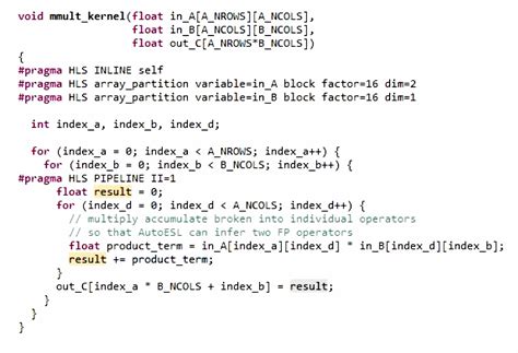
- High-Level Synthesis (HLS): Generating HDL from C/C++ specifications
- Partial Reconfiguration: Modifying a portion of the FPGA logic while the rest remains active
- External Memories: Interfacing with DDR, HBM or other high-speed RAM
- DSP Blocks: Using hardened multiply-accumulate units for digital signal processing
- Debugging: Using integrated logic analyzers and virtual I/O to debug problems
Frequently Asked Questions (FAQ)
1. What coding language is used for FPGA programming?
FPGA programming typically uses hardware description languages (HDLs) like Verilog and VHDL. These languages allow you to describe the desired digital logic circuits at a register-transfer level (RTL) of abstraction. High-level synthesis (HLS) tools also allow FPGAs to be programmed using C/C++ or SystemC.
2. Is FPGA programming hard?
FPGA programming requires a mix of hardware and software skills. You need to understand digital logic design concepts as well as the syntax and constructs of HDLs. Getting used to the FPGA vendor tools and board-level implementation can also take some practice. However, with good learning resources and practical experience, FPGA programming can be mastered by dedicated students and engineers.
3. How much does an FPGA development board cost?
FPGA development board prices vary widely depending on the FPGA size, speed grade, and peripherals included. Simple boards for beginners can cost under $100, while high-end boards with the largest and fastest FPGAs can be tens of thousands of dollars. For most projects, a mid-range board in the $200 to $1000 range is sufficient.
4. What are the advantages of FPGA over microcontroller?
FPGAs offer several advantages over microcontrollers for certain applications:
– Parallel processing: FPGAs can implement many independent digital logic circuits operating simultaneously, while microcontroller execute a sequential program
– Customization: FPGAs can be programmed to implement custom digital logic tailored for a specific application
– Timing control: FPGAs offer precise control over signal timing and can achieve higher clock rates than most microcontrollers
– Interfacing: FPGAs can directly interface with high-speed peripherals and protocols
However, microcontrollers are generally lower cost, lower power, and easier to program for control-dominated applications.
5. What companies make FPGAs?
The main FPGA vendors are:
– Xilinx (now part of AMD)
– Intel (acquired Altera)
– Lattice Semiconductor
– Microchip (acquired Microsemi)
– QuickLogic
Xilinx and Intel (Altera) FPGAs are most commonly used, but each vendor offers unique devices and tools targeting different applications and price points.
In summary, FPGA programming is a powerful skill for implementing custom digital logic on reconfigurable hardware. By learning HDLs, mastering the programming flow, and practicing with development boards, you can start unlocking the potential of FPGAs for your projects. While the learning curve can be steep, the rewards in terms of performance, flexibility and rapid prototyping are well worth the effort.


Leave a Reply